
 LOGIN
LOGIN Downloads


1. Library Editor
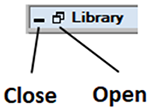
Open the FPX file half screen with the first click. Full screen with the second click.
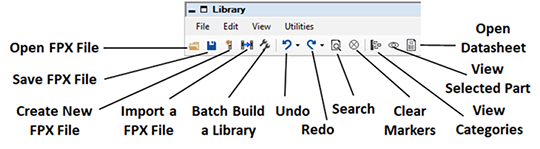
2. Library Toolbar
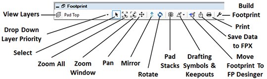
3. Footprint Toolbar
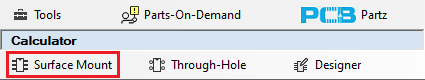
4. Surface Mount Calculators
Left Mouse Click "Surface Mount"
Select a component family by Double Click on the line or select the line and select the "OK" button.
There are 44 main Surface Mount component families and 121 subfamilies.
1. Ball Grid Array (BGA)
2. Capacitor, Aluminum Electrolytic
3. Ceramic Flat Pack (CFP)
4. Ceramic Flat Pack (CQFP)
5. Chip
a. Antenna
b. Capacitor
c. Capacitor, Polarized
d. Choke
e. Crystal
f. Diode
g. Diode (non-polarized) or Unidirectional
h. Ferrite Bead
i. Filter
j. Fuse
k. Inductor
l. LED
m. Resistor
n. Thermistor
o. Varistor
6. Chip Array, 2 Side Flat/Concave
a. Capacitor
b. Choke
c. Diode
d. Ferrite Bead
e. Filter
f. Inductor
g. Integrated Circuit
h. Oscillator
i. Resistor
7. Chip Array, 2 Side Convex
a. Capacitor
b. Choke
c. Inductor
d. Oscillator
e. Resistor
8. Chip Array, 4 Side Flat/Concave
a. Capacitor
b. Choke
c. Diode
d. Ferrite Bead
e. Filter
f. Inductor
g. Oscillator
h. Resistor
9. Column Grid Array (CGA)
10. Corner Concave Crystal/Oscillator
a. Crystal
b. Oscillator
11. SMD Crystal
12. Dual Flat No-Lead (DFN) 2 Pins
a. Antenna
b. Capacitor
c. Capacitor, Polarized
d. Crystal
e. Diode
f. Diode (non-polarized) or Unidirectional
g. Filter
h. Fuse
i. Inductor
j. Resistor
k. Thermistor
l. Varistor
13. Dual Flat No-Lead (DFN) 3 Pins
a. Antenna
b. Capacitor
c. Choke
d. Diode
e. Ferrite Bead
f. Filter
g. Inductor
h. IC (integrated Circuit)
i. Resistor
j. Thermistor
k. Transistor
l. Varistor
14. Dual Flat No-Lead (DFN) 4 Pins
a. Antenna
b. Capacitor
c. Choke
d. Crystal
e. Diode
f. Ferrite Bead
g. Filter
h. Inductor
i. IC (integrated Circuit)
j. Oscillator
k. Resistor
l. Thermistor
m. Transistor
n. Varistor
15. DPAK
16. Leadless Chip Carrier
17. Land Grid Array (LGA)
18. Metal Electrode Leadless Face (MELF)
a. Diode
b. Diode, Non-polarized
c. Fuse
d. Resistor
19. Molded Body
a. Capacitor
b. Capacitor, Polarized
c. Choke
d. Diode
e. Diode, Non-polarized
f. Ferrite Bead
g. Filter
h. Fuse
i. Inductor
j. Inductor, Polarized
k. LED
l. Resistor
m. Thermistor
n. Thyristor
o. Varistor
20. Oscillator, J-Lead
21. Oscillator, L-Bend
22. Oscillator, Side Concave
23. Plastic Leaded Chip Carrier (PLCC)
24. Quad Flat Pack (QFP)
25. Quad Flat Pack (QFP) with Tab
26. Quad Flat No-Lead (QFN)
a. D-Shape (Lead Shape)
b. Rectangular (Lead Shape)
27. Quad Flat No-Lead (QFN) with Tab
a. D-Shape (Lead Shape)
b. Rectangular (Lead Shape)
28. Pullback Quad Flat No-Lead (PQFN)
a. D-Shape (Lead Shape)
b. Rectangular (Lead Shape)
29. Pullback Quad Flat No-Lead (PQFN) with Tab
a. D-Shape (Lead Shape)
b. Rectangular (Lead Shape)
30. Pullback Small Outline No-Lead (PSON)
a. D-Shape (Lead Shape)
b. Rectangular (Lead Shape)
31. Pullback Small Outline No-Lead (PSON) with Tab
a. D-Shape (Lead Shape)
b. Rectangular (Lead Shape)
32. Side Concave Package
33. Small Outline Diode (SOD)
a. Diode
b. Diode, Non-polarized
34. Small Outline Diode Flat Lead (SODFL)
a. Diode
b. Diode, Non-polarized
35. Small Outline Flat Lead (SOFL)
a. Diode
b. Filter
c. Integrated Circuit
d. Transformer
e. Transistor
36. Small Outline J-Lead (SOJ)
37. Small Outline L-Lead (SOL)
38. Small Outline No-Lead (SON)
a. D-Shape (Lead Shape)
b. Rectangular (Lead Shape)
39. Small Outline No-Lead (SON) with Tab
a. D-Shape (Lead Shape)
b. Rectangular (Lead Shape)
40. Small Outline Package (SOIC, SOP)
41. Small Outline Package (SOIC, SOP) with Tab
42. Small Outline Transistor (SOT23)
43. Small Outline Transistor (SOT143)
44. Small Outline Transistor (SOT223)
5. Through-hole Calculators
Left Mouse Click "Through-hole"
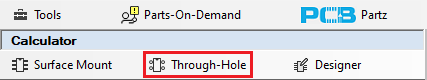
Select a component family by Double Click on the line or select the line and select the "OK" button.
There are 25 main Through-hole component families and 41 subfamilies.
1. Axial
a. Capacitor
b. Capacitor, Polarized
c. Diode
d. Diode, Non-polarized
e. Fuse
f. Inductor
g. Resistor
2. Dual-In-Line Package (DIP)
3. Dual-In-Line Package (DIP Socket)
4. Header, Right Angle, Post
5. Header, Right Angle, Receptacle
6. Header, Right Angle, Shrouded
7. Header, Vertical (All Types)
a. Non-shrouded
b. Header, Vertical, Shrouded
c. Header, Vertical, Receptacle
8. Mounting Hole
9. Oscillator
10. Pin Grid Array (PGA)
11. Radial (Dipped) round
a. Capacitor
b. Capacitor, Polarized
12. Radial (Dipped) rect.
a. Capacitor
b. Capacitor, Polarized
c. Fuse
d. Resistor
13. Radial (Dipped) with offset leads
a. Capacitor
b. Fuse
c. Resistor
14. Radial (Disk)
a. Capacitor
b. Fuse
c. Resistor
d. Thermistor
e. Varistor
15. Radial (Disk) with offset leads
a. Capacitor
b. Fuse
c. Resistor
d. Thermistor
e. Varistor
16. Radial (Electrolytic)
a. Capacitor
b. Capacitor, Polarized
17. Radial (Inductor)
a. Inductor
b. Inductor, Polarized
18. Radial (Molded)
a. Capacitor
b. Fuse
c. Inductor
d. Resistor
19. Radial (LED) round
a. Rectangle (Lead Shape)
b. Round (Lead Shape)
20. Radial (LED) rect.
a. Rectangle (Lead Shape)
b. Round (Lead Shape)
21. Single-In-Line Package (SIP)
22. TO-92
23. Flange Mounted (TO) horiz.
24. Flange Mounted (TO) vert.
25. TO Cylindrical Style
6. Calculator Buttons

Clear Entries is used to remove all package dimensions from the calculator cells.
Clear and Reset Options are also used to remove any settings that were manually changed in these panels:
- Options
- 3D Colors
- Terminal Density Level
- Pad Stack Rules
- Drafting Options
- Footprint - Manufacturer's Recommended Pattern
Demo is used to fill in all the package dimensional data for the footprint displayed in the viewer.
The Demo button is normally used for testing purposes and the dimensional data does not relate to a real part.
The Calculate button is selected after all min/max cells are completed. If you missed a package dimension, the calculator will auto-generate a warning icon by the missing dimension required to generate the footprint.
The Add to Library button is used to add the dimensions to the FPX library.
