
 LOGIN
LOGIN Downloads


Welcome to the next generation of PCB library development. The Footprint Expert is the original IPC footprint automation solution, which is also flexible enough for the most advanced user-defined modifications to effortlessly create footprints from component data. It outputs individual parts or entire libraries to all major CAD formats (each available separately). Here is what you get with the CAD output for Altium Designer license:
- Output to format readable by Altium Designer
- Supports Altium Designer
- Our advanced CAD LEAPTM Technology
(Libraries Enhanced with Automated Preferences) - IPC J-STD-001 Compliant solder joint goals
- IPC-7352 & IPC-7351 Compliant calculations and naming conventions
- IEC 61188-7 Compliant Default Zero Component Orientation
- Parts on Demand 2+ million parts starter library
- BOM Builder Service (POD Credits optional purchase)*
- New part requests, regardless complexity, as little as $5 each**
- 12 Months of updates included!
- Ability to create footprints with arbitrary pad shapes and positions
- Enter component dimensions using Nominal plus tolerance or Min/Max dimensions
- Pin rename & renumber
- Automate creation of component manufacturer recommended footprints
- One-click rotate/mirror footprint, very useful for rapid LGA/BGA design
- One-click pad shapes supported: Rectangle, Oblong, D-Shape, and Rounded Rectangle
- Dynamic support for Imperial and metric - easily convert between mil and metric units
- Convert units calculator
- Apply rules to component families and component terminal lead types
- User friendly GUI easy to learn
- Padstack editor
- FREE training webinars as needed, one-on-one or group
- High priority phone, email, or shared desktop support
- Low cost & FASTEST return on investment
- Perpetual license does not expire; no maintenance
- Add and modify library documentation
- User definable preferences or define and customize default rules
- Save component dimensions to a library file
- Search, edit, save functions for effective part library management
- Flexibility to add, delete, or modify data fields - for example:
- Corporate Part Number
- Schematic Symbol Name
- Created By / Date
- Purchased From
- Bulk / Piece Price
- DigiKey Part Number
- Project Name
- etc... (no limit!)
** New part requests start at $10, per pricing schedule posted on POD credits page.
We built the Footprint Expert around the notion that there are as many unique PCB library needs as there are users.
If you consider tolerance settings, units, line-widths, pad shapes, rotations, and many dozens of other settings (all configurable with the PCB Footprint Expert), you can create over 1,800 variations of ONE SINGLE library! We empower you to quickly build high-quality standard libraries to meet your specific needs.
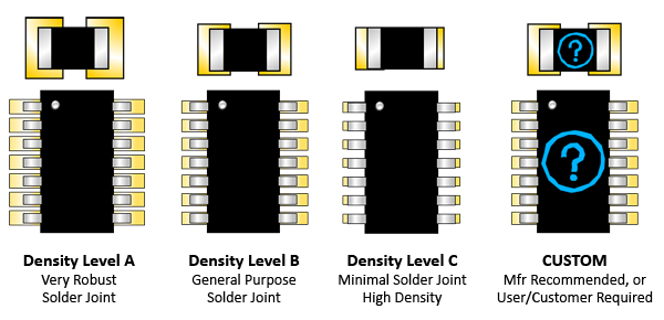
5-Tier Density Variations Supported
![]() 1IPC A: Maximum (Most) Land Protrusion – For low-density product applications, the 'maximum' land pattern condition has been developed to accommodate wave or flow solder of leadless chip devices and leaded gull wing devices. The geometry furnished for these devices, as well as inward and "J" - formed lead contact device families, may provide a wider process window for reflow solder processes as well.
1IPC A: Maximum (Most) Land Protrusion – For low-density product applications, the 'maximum' land pattern condition has been developed to accommodate wave or flow solder of leadless chip devices and leaded gull wing devices. The geometry furnished for these devices, as well as inward and "J" - formed lead contact device families, may provide a wider process window for reflow solder processes as well.
2IPC B: Median (Nominal) Land Protrusion – Products with a moderate level of component density may consider adapting the 'median' land pattern geometry. The median land patterns furnished for all device families will provide a robust solder attachment condition for reflow solder processes and should provide a condition suitable for wave or reflow soldering of leadless chip and leaded Gull Wing type devices.
3IPC C: Minimum (Least) Land Protrusion – High component density typical of portable and hand-held product applications may consider the 'minimum' land pattern geometry variation. Selection of the minimum land pattern geometry may not be suitable for all product use categories. The use of classes of performance 1, 2, and 3 is combined with that of component density levels A, B, and C in explaining the condition of an electronic assembly. As an example, combining the description as Levels 1A or 3B or 2C, would indicate the different combinations of performance and component density to aid in understanding the environment and the manufacturing requirements of a particular assembly.
4User-defined preferences. Companies can establish a standard set of preferences to apply to all users of the PCB Footprint Expert! Settings include:
|
5
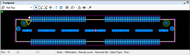
Component manufacturer-recommended footprint.
![]()
 The Footprint Expert is synchronized to the latest guidelines of the IPC-7352, IPC-7351, and IPC-J-STD-001 (Requirements for Soldered Electrical and Electronic Assemblies). You want your PCB Layout to pass the J-STD-001 standard for solder joint acceptability in the PCB assembly process. You also get the ability to migrate your entire library to future revisions or your own custom-defined requirements as well! Why is this important? Because it ensures that everybody - regardless of experience or language - can build high-quality parts in the same standard, professional way!
Improve your PCB Library skills with solder joint goal knowledge. Take the IPC-J-STD-001 training class ASAP! The PCB designer and EE engineer should have as much information about the PCB assembly process as possible for DFA (Design for Assembly).
We have been involved in IPC standards development for many years, and are intimately familiar with the IPC-7352, IPC-7351, and J-STD-001.
The Product Sheet (PDF) is available in a few languages:


Download and install the Evaluation License for the PCB Footprint Expert to see for yourself how it can benefit you! Feel free to contact us or any of our world-wide distributors with questions or to request no-obligation demos!
There are seven types of licenses:
- Single User USB Key (perpetual)
- Network USB Key (perpetual)
- Global Network USB Key (perpetual)
- Single User SL (12-month based refresh)
- Network SL (12-month based refresh)
- Global Network SL (12-month based refresh)
- Lease License (with MAC address limit)
By default, all quotes issued are for the perpetual USB Key, our most popular configuration. Users who want to go without a USB Key (for example if installing a Network License on a virtual server), have the option of the SL license.
See available license options summarized here.
Leased License (Cloud)
Two types of Leased Licenses are available 1) Regular, which may be shared on company site, or by employees working from home within 100 miles / 161 kilometers from company site, and 2) Global, which may be shared with other company users globally. The Lease License is available in monthly and annual increments, with access limited by quantity of MAC addresses purchased. The availability of this license is subject to a number of variables such as internet connectivity, firewall settings, etc.
PCBL may impose other restrictions for users of the Leased License, such as Software upgrade requirements, meaning you will need to upgrade to keep using the Software. Availability of this license is subject to numerous variables related to network/internet connectivity between you and PCBL servers, as well as downtime due to other reasons - such downtime for updates or maintenance. Proxy Servers are not supported.
Single User License (USB Key)
This perpetual license entitles you to install and run the software on one local computer. This solution is ideal for the PCB design contractor or companies with one PCB designer. The Single User is licensed on USB key, and can be easily moved to any computer as needed. Contracting and/or always changing computers? No problem, we make it a snap!!
Network License (USB Key)
 The Network License is perpetual and available for all the users you need! It is ideal where library standardization is desired, regardless the CAD formats used. Professionals or novices can now easily create libraries according to company specification and customer requirements. The Network License is based on a network-enabled USB key that may be placed on a server or even a regular/user's computer. Once configured, when a user on the network opens the Footprint Expert, a license is automatically checked out from the key. When the Footprint Expert is closed, the license is made available for others to check out.
Global Network License (USB Key)
The Global Network License is identical to the Network License, but in addition also gives customer right to place the Network License on the company's globally-accessible network so it is available to company users outside the location assigned to the license, via a secured Virtual Private Network (VPN).
Single-SL, Network-SL, and Global-Network-SL Licenses
The HASP "SL" Licenses (Single and Network) are not perpetual and expire 12 months after purchase, at which time they cease to function unless they either get Refreshed or Replaced.
- Refresh - renewing same License ID (on same machine, or server if a network license)
- Replace - issue a new License ID for a new PC or server
 There will be no cost to REFRESH nor REPLACE either SL license if in conjunction with a software maintenance purchase. If no software maintenance is purchased, and the license needs to be refreshed for a Footprint Expert version that is no longer on active software maintenance, the 12-month REFRESH will be subject to a non-refundable processing fee of $100. THERE IS NO GUARANTEE that older versions of the Footprint Expert will function as intended - or at all - with newer operating systems, patches, .NET Framework updates, etc.
If the license needs to be installed on a new computer or a new activation is required for whatever reason, a REPLACEMENT license will be required, and will be subject to a non-refundable processing fee of $125; customer and PCBL may need to take steps to terminate all previously issued license(s)/activation(s) that are being replaced. A limit of 3 license replacements are allowed for each VERSION of the Footprint Expert for which a license is purchased, after which the licenses must be repurchased.
NOTE: All costs associated with REFRESH or REPLACEMENT of SL Licenses are subject to reasonable change year to year.
User Accounts
User Accounts are needed to login and download the latest release of the Footprint Expert, as well as access POD. User Accounts are limited to one (1) per Single User License, and three (3) for Network Licenses. Footprint Expert Enterprise users may consider POD Subscriptions - online part data that complements the Footprint Expert software, and many users purchase together.
Risk-free Purchase
Before you purchase anything, you can evaluate the software to see how it works for you. It only takes minutes to evaluate! Contact Us if you have any questions or prefer a walk-through!
System Requirements
 Microsoft Windows based computer, running Windows 11 (Windows 10, 8, 7, and XP will likely still work, but are no longer supported by Microsoft); the Microsoft .NET Framework 4.0 (downloadable from Microsoft), 40MB of hard drive space, a USB port (if using the USB Key edition), and display resolution of 1024 x 768. The Footprint Expert is also known to work on Linux machines if using a Windows emulator (eg., Wine), however we can provide very limited support in this regard.
Our solutions are used by individuals at these companies, and many thousands more:


![]()


Get a 30-DAY EVALUATION!
Select type of license:

"FREE" Cloud License
Just pay maintenance equivalent of Single User license - same as 80% OFF!


 Also interested in 3D STEP or multiple licenses? Contact us!
SEE SAMPLE FILES
Download and install the Evaluation License for the PCB Footprint Expert to see for yourself how it can benefit you! Feel free to contact us or any of our world-wide distributors with questions or to request no-obligation demos!

We developed the industry's original IPC-7351 footprint calculator!