LOGIN
LOGIN Downloads


KiCad is a tool in constant development. As such, certain key functionality that can be found in other CAD tools simply does not yet exist in KiCad. With the exception of the following five issues, at this present time, KiCad library automation is fairly thorough and powerful enough to save you lots of time. To avoid issues, please make sure to use the KiCad preference file - "IPC-7351B KiCad.dat".
1. Rounded Rectangles - Put quite simply, they do not exist, nor are there any facilities to mimic them. As such, any and all Rectangles with Rounded corners will have their corners straightened on translation. The length and width of the overall rectangle should remain the same.
2. Copper Areas - These also do not exist and any copper area in your FPX part (particularly out of FP Designer), will not translate.
3. Paste Mask Checkerboard - Checkerboard is typically done by areas of copper on layers that are not electrical (i.e. Paste mask). As no facilities exist, any part with a thermal tab that has a paste mask checkerboard will translate as a thermal tab without paste mask. The user will need to adjust this as desired as part of the post-process.
4. Keep-outs - KiCad 'Legacy' versions do not support these, so any keep-outs will not be translated.
5. Layer names cannot be changed.
6. Design Units - KiCad footprint (*.kicad_mod) files only support millimeters. Therefore, all parts constructed for translation to KiCad must be in millimeters. Data may be input in other units but must be converted (using Component Data/Options) before translation to KiCad. If 'batch-building' parts from a library, ensure Millimeters are selected as the default for Design Units. Note: There are no warning or error message alerts if other units are selected but the translated footprint will appear distorted.
IMPORT INSTRUCTIONS
* Ensure the selected translator version matches your CAD software version.
1. Double Click to open any part in any FPX file.
2. Select the Build Part  or Build
Library
or Build
Library ![]() icon
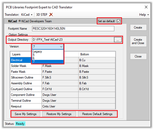
in Footprint Expert and in the Create Footprint menu select the Translator
KiCad, Set as Default Format, create an output Directory and select "Save My Preferences".
icon
in Footprint Expert and in the Create Footprint menu select the Translator
KiCad, Set as Default Format, create an output Directory and select "Save My Preferences".
3. Select the "Create and Close" button:
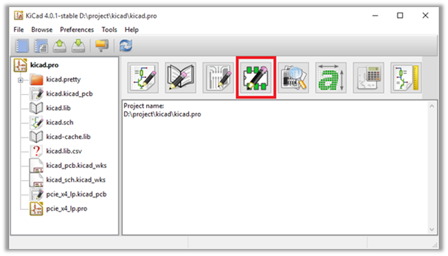
4. You should see the following window. Click on the PCB Footprint Editor button highlighted in red.
5. You should see the following Footprint Editor Window. To load a .kicad_mod file created by the Footprint Expert tool select File -> Load Footprint -> Import Footprint from File.
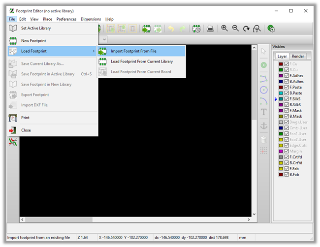
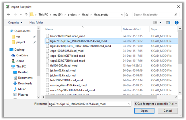
6. Browse to where you generated the .kicad_mod file, select it, and open it.
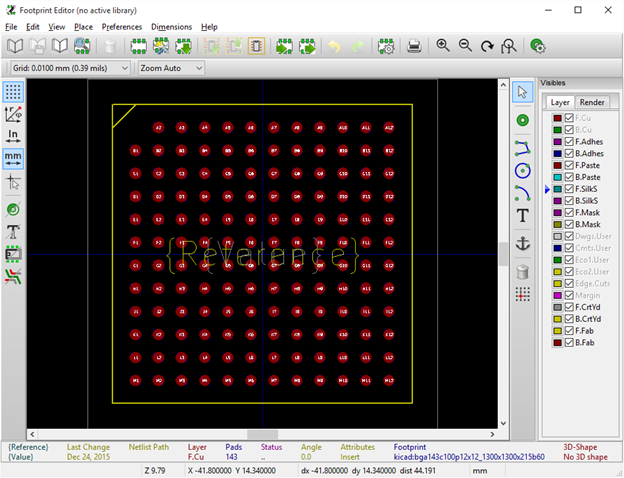
7. Your part should now be fully imported into the KiCad Footprint Editor.