
 LOGIN
LOGIN Downloads


After entering the package dimensions in the Body
Outlines panel, selecting the OK button will automatically collapse the Body
Outlines panel and open the Pad Stack Designer menu.
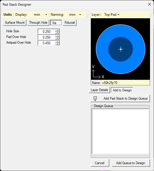
The Pad Stack Designer creates all the necessary pad stacks for the footprint.
At the top of the menu is "Units" and there are 2 options.
- Display:
- mm
- um
- Inch
- Mils
Display units are for entering pad stack values.
- Naming:
- mm
- Mils
Naming units creates the pad stack name in mm or mil units.
The Display and Naming combinations provide flexibility when switching between units.
Create pad stacks for:
- Surface Mount
- Through-hole
- Via
- Fiducial
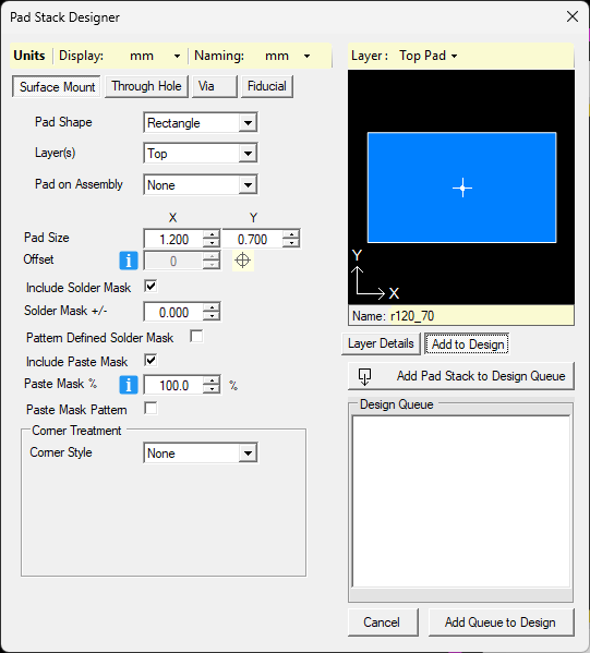
Surface Mount options:
Pad Shape:
- Round
- Oblong
- Square
- Rectangle
- D-Shape
Layers:
- Top
- Bottom
- Top and Bottom
Pad on Assembly:
- None
- Filled
- Outline
Pad Size: X & Y - Note: X should be the longest dimension.
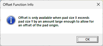
Offset:
Include Solder Mask: check box for Yes.
Solder Mask +/-: this is the annular ring.
Pattern Defined Solder Mask: check box for Yes.
This feature is used for a Thermal Pad to make the solder mask aperture the same size as the paste mask aperture. This feature is referred to as a Solder mask Defined Thermal Pad.
Include Paste Mask: check box for Yes.
Paste Mask %: 100% is normal for pad stacks and 60% is the average for Thermal Pad Paste Mask reduction. Thermal paste mask reduction is normally between 50 - 70%.
Paste Mask Pattern: check box for Yes.
Corner Treatment:
Corner Styles:
- None
- Radius
- Chamfer
- Both
None will produce a rectangular pad shape.
Radius is a corner radius that can be on these corners:
- All
- Top
- Left
- Right
- Bottom
Chamfer is a 45-degree corner that can be on these corners:
- All
- Top
- Left
- Right
- Bottom
Both options are a combination of a Chamfer on one corner and radius on the other 3 corners.
Feature Locations: (this is for the Chamfer)
- Upper Left
- Upper Right
- Lower Left
- Lower Right
Note: use 'Both' to create a Chamfered SMD pad on one corner. Make the radius value 0.00.
Through Hole options:
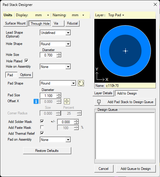
Lead Shape (Optional):
- Undefined
- Round
- Square
- Rectangle
Hole Shape:
- Round
- Slot
Hole Size:
- Round = Diameter
- Slot = X (Length) Y (Width)
Hole Plated: check box for Yes. Unchecking this box will create a non-plated hole.
Hole on Assembly:
- None
- Filled
- Outline
Pad:
Pad Shape:
- Round
- Oblong
- Square
- Rounded Square
- Rectangle
- Rounded Rectangle
Pad Size: Diameter - Value
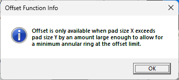
Offset X:
Include Solder Mask: check box for Yes.
Solder Mask +/-: annular ring value.
Include Paste Mask: check box for Yes.
Pad on Assembly:
- None
- Filled
- Outline
Thermal Relief: check box for Yes. Unchecking this box will create a direct connection to the plane.
Via options:
- Hole Size: value
- Pad Over Hole: value – this setting is the annular ring
- Antipad Over Hole: value – this setting is the plane clearance
Fiducial options:
- Pad Shape
- Round
-Square - Pad Size: value - the value range is from 0.50 to 1.50
- Used for both local and global fiducials - Solder Mask Size: value - the value is typically 2X the pad size
- Keepout Size: value - the keepout size is typically the same size as the solder mask
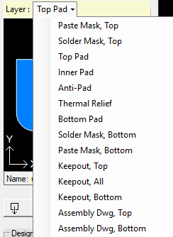
After entering all the values for a pad stack, select the Layer dropdown to view the layers.
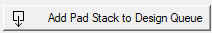
After reviewing the layers, select, the 'Add Pad Stack to Design Queue' button.
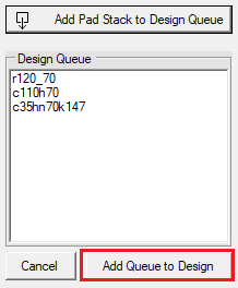
Create any remaining pad stacks and select the 'Add Pad Stack to Design Queue' button for each one.
When all the pad stacks are in the Design Queue, select the 'Add Queue to Design' button.
When the 'Add Queue to Design' button is selected, the Pad Stack Manager will automatically open.
