
 LOGIN
LOGIN Downloads


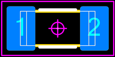
This is an example of a 1206 Chip Resistor package.
Dimensions: H = 1.40, D = 3.20 ±0.20, E = 1.60 ±0.20, L = 0.50 ±0.25
The IPC-7352 mathematical model includes the D, E and L dimensions and tolerances and the solder joint goal settings for Toe = 0.35, Heel = 0.00, Side = 0.00
Resulting pad size rounded to 2 places is L 1.15 x W 1.80 x G 1.80
The resulting pad stack pattern must have the terminal leads on the pad stack in these conditions:
1. The Nominal Material condition of the component package & Nominal Terminal.

2. The Minimum Material condition of the component package & Nominal Terminal.

3. The Maximum Material condition of the component package & Nominal Terminal.

4. The Minimum Material condition of the component package & Minimum Terminal.
5. The Maximum Material condition of the component package & Maximum Terminal.

The resulting pad stack must have terminal leads on the pad stack regardless of every possible Material Condition possible to pass assembly inspection and meet the requirements set forth in the IPC J-STD-001 Standard and the IPC-7352 Guideline in Figure 3-3 Profile Dimensioning.
i.e.: regardless of the Component Package and Terminal Lead Material Condition, the Terminal Lead must never be exposed outside the calculated pad stack.
This is proof that the V24 Footprint Expert mathematical model illustrated in the IPC-7352 guideline achieves that goal.
Note: most component packages are created in the Nominal Material Conditions. The package tolerances play a key role in the resulting pad stack.
This footprint image represents Nominal Package Dimensions with no Package Tolerances:

The Footprint Expert uses the IPC-7352 Mathematical Model.
