

|
|
SODFL & SOTFL |
Post Reply 
|
| Author | |
Tom H 
Admin Group 

Joined: 05 Jan 2012 Location: San Diego, CA Status: Offline Points: 6069 |
 Post Options Post Options
") Thanks(0) Thanks(0)
 Quote Reply Quote Reply
 Topic: SODFL & SOTFL Topic: SODFL & SOTFLPosted: 26 Nov 2024 at 11:23am |
|
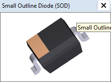
SOD is Gull Wing leads:
 SODFL is Flat Leads: 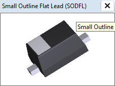 BTC (Bottom Terminal Component) = QFN, SON, PQFN, PSON, BGA, LGA. CGA, etc. |
|
 |
|

|
|
|
|
|
MGOS
New User 
Joined: 23 Oct 2024 Status: Offline Points: 6 |
Post Options
Thanks(1)
Quote Reply
Posted: 23 Oct 2024 at 1:39am |
Apologies
for hijacking this thread, but I'd rather ask here then create a new
thread for the same SODFL package type, if that is OK.
I have some difficulties classifying this type of components as to IPC standard (IPC-A-610J, class 3); mainly, is there a definite type to which they belong and I can check during PCB inspection? For instance, based on figures and specs I could classify as:
I know text has precedence to images that is why I am asking this to finally sort this out for me. Thank you for information. |
|
|
|
|
mohamedjubair.k
Active User 
Joined: 05 Sep 2022 Status: Offline Points: 26 |
Post Options
Thanks(0)
Quote Reply
Posted: 05 Mar 2023 at 8:53am |
|
Thank you so much Tom!
|
|
|
|
|
Tom H
Admin Group
Joined: 05 Jan 2012 Location: San Diego, CA Status: Offline Points: 6069 |
Post Options
Thanks(0)
Quote Reply
Posted: 04 Mar 2023 at 9:45am |
|
It's the same concept. You take the "Nominal c" dimension (and round up to the nearest 0.05) and that is your Toe goal.
Anything bigger than that is a waste of PCB real-estate and excess solder. The main strength in the solder joint is under the terminal lead. 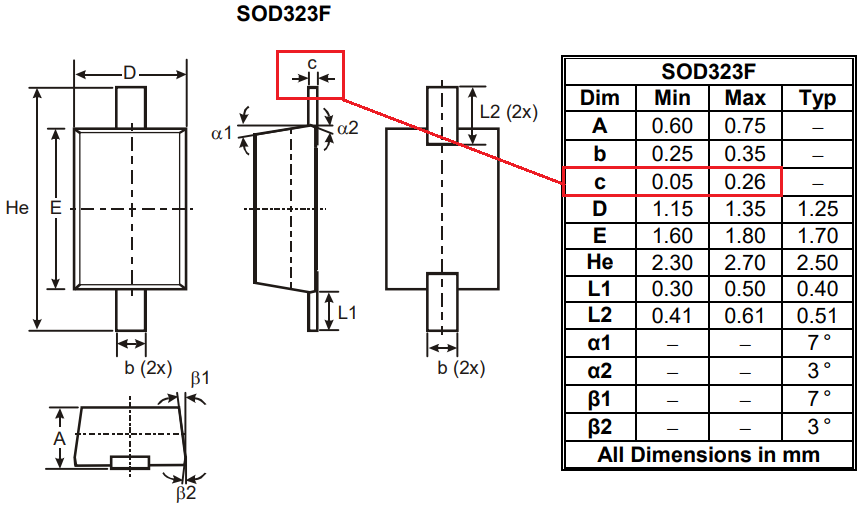 |
|
|
|
|
mohamedjubair.k
Active User
Joined: 05 Sep 2022 Status: Offline Points: 26 |
Post Options
Thanks(0)
Quote Reply
Posted: 03 Mar 2023 at 6:10pm |
|
Hi Tom,
Thank you for you quick reply. Actually I need information about Flat Lead component like attached. 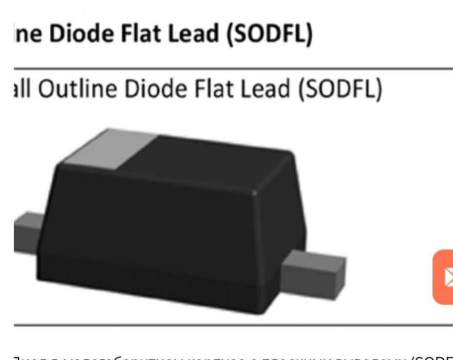 |
|
|
|
|
Tom H
Admin Group
Joined: 05 Jan 2012 Location: San Diego, CA Status: Offline Points: 6069 |
Post Options
Thanks(0)
Quote Reply
Posted: 03 Mar 2023 at 8:59am |
|
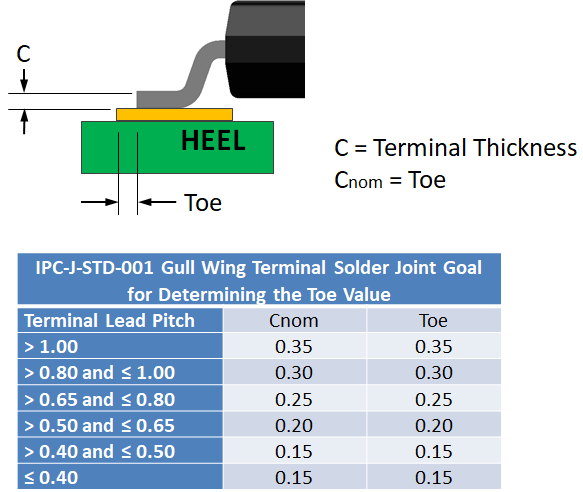
Per IPC J-STD-001 Standard, the Toe value is determined by the Terminal Lead Thickness.
This is the example of the Gull Wing Terminal Lead form.
 |
|
|
|
|
mohamedjubair.k
Active User
Joined: 05 Sep 2022 Status: Offline Points: 26 |
Post Options
Thanks(0)
Quote Reply
Posted: 03 Mar 2023 at 4:13am |
|
Hi Tom,
I read the IPC-7351 document and I did not see solder joint goal table for flat leads [SODFL and SOTFL] components. But in library calculator Toe joint value found as 0.20 mm. From where did they find this value. Is this 0.20 mm is fine for Toe end. 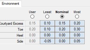 |
|
|
|
|
Post Reply
|
|
| Tweet |
| Forum Jump | Forum Permissions You cannot post new topics in this forum You cannot reply to topics in this forum You cannot delete your posts in this forum You cannot edit your posts in this forum You cannot create polls in this forum You cannot vote in polls in this forum |


 Topic Options
 Tom H wrote: