
|
|
Three-Tier Density Levels |
Post Reply 
|
| Author | |||||||||||||||||||||||||||||||||
Nick B 
Admin Group 

Joined: 02 Jan 2012 Status: Offline Points: 2066 |
 Post Options Post Options
 Thanks(0) Thanks(0)
 Quote Reply Quote Reply
 Topic: Three-Tier Density Levels Topic: Three-Tier Density LevelsPosted: 15 Aug 2026 at 11:00am |
||||||||||||||||||||||||||||||||
|
Performance classification: IPC J-STD-001, formally titled "Requirements for Soldered Electrical and Electronic Assemblies," is the global industry standard for soldering materials and processes. Unlike other standards that focus solely on visual inspection, J-STD-001 emphasizes process control, ensuring that the assembly is built correctly from the start.
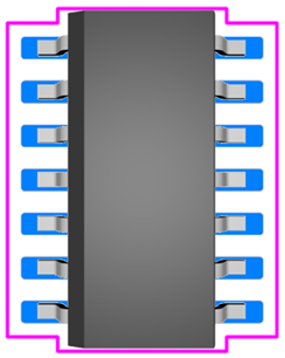
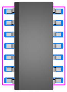
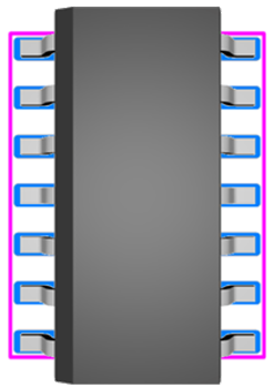
Classification: Products are divided into three classes based on their criticality: CLASS 1 General Electronic Products Includes products suitable for applications where the major requirement is function of the completed assembly. CLASS 2 Dedicated Service Electronic Products Includes products where continued performance and extended life are required, and for which uninterrupted service is desired but not critical. Typically, the end-use environment would not cause failures. CLASS 3 High Performance Electronic Products Includes products where continued high performance or performance-on-demand is critical, equipment downtime cannot be tolerated, end-use environment may be uncommonly harsh, and the equipment must function when required, such as life support or other critical systems. The use of performance classes (1, 2, and 3) is combined with that of component density levels (A, B, and C) in explaining the condition of an electronic printed board assembly. As an example, combining the description as Levels 1A or 3B or 2C, would indicate the different combinations of performance and component density to aid in understanding the environment and the manufacturing requirements of a particular printed board assembly. The Three Density Levels
Select the correct level depending on your target manufacturing capability and the physical size constraints of your PCB. Using tools like the free PCB Libraries Footprint Expert Calculator or the Footprint Expert can help automatically generate these patterns based on component dimensions.
Summary of Differences
|
|||||||||||||||||||||||||||||||||
 |
|||||||||||||||||||||||||||||||||

|
|||||||||||||||||||||||||||||||||
|
|||||||||||||||||||||||||||||||||
|
Post Reply
|
|
| Tweet |
| Forum Jump | Forum Permissions You cannot post new topics in this forum You cannot reply to topics in this forum You cannot delete your posts in this forum You cannot edit your posts in this forum You cannot create polls in this forum You cannot vote in polls in this forum |


 Topic Options