|
Performance classification: IPC J-STD-001, formally titled "Requirements for Soldered Electrical and Electronic Assemblies," is the global industry standard for soldering materials and processes. Unlike other standards that focus solely on visual inspection, J-STD-001 emphasizes process control, ensuring that the assembly is built correctly from the start. - Materials & Equipment: Specifies acceptable types of solder (both leaded and lead-free), flux, adhesives, and tools like soldering irons or rework stations.
- Soldering Processes: Covers methods for manual, wave, and reflow soldering, including specific requirements for component mounting and hole fill.
- Verification & Cleaning: Defines cleanliness testing and inspection methodology to ensure assemblies are free from harmful contaminants.
Classification: Products are divided into three classes based on their criticality:
CLASS 1 General Electronic Products Includes products suitable for applications where the major requirement is function of the completed assembly.
CLASS 2 Dedicated Service Electronic Products Includes products where continued performance and extended life are required, and for which uninterrupted service is desired but not critical. Typically, the end-use environment would not cause failures.
CLASS 3 High Performance Electronic Products Includes products where continued high performance or performance-on-demand is critical, equipment downtime cannot be tolerated, end-use environment may be uncommonly harsh, and the equipment must function when required, such as life support or other critical systems.
The use of performance classes (1, 2, and 3) is combined with that of component density levels (A, B, and C) in explaining the condition of an electronic printed board assembly.
As an example, combining the description as Levels 1A or 3B or 2C, would indicate the different combinations of performance and component density to aid in understanding the environment and the manufacturing requirements of a particular printed board assembly.
The Three Density Levels - Density Level A: Maximum (Most) Land Protrusion
- IPC Designation: M (for Maximum footprint).
- Characteristics: Provides the largest Pad size and Courtyard area and most robust solder joints.
- Applications: Suitable for prototypes, low-density boards, or products subjected to high shock or vibration. It offers a wider "process window," making it the most rework-friendly level.
- Density Level B: Median (Nominal) Land Protrusion
- IPC Designation: N (for Nominal footprint).
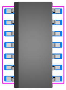
- Characteristics: A balanced middle ground between board density and manufacturing robustness. Average Pad size and Courtyard area.
- Applications: The standard choice for most general-purpose commercial electronics. It provides stable solder attachments for typical reflow and wave soldering processes.
- Density Level C: Minimum (Least) Land Protrusion
- IPC Designation: L (for Least footprint).
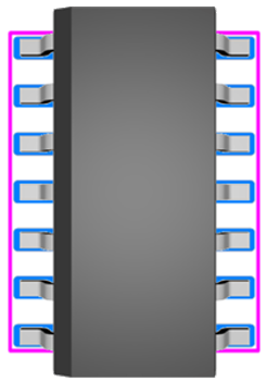
- Characteristics: Uses the smallest Pad size and Courtyard area and courtyard area to achieve maximum component packing density.
- Applications: Essential for space-constrained designs like mobile phones, handheld medical devices, and HDI (High-Density Interconnect) boards. Due to the small pads, rework is difficult.
Select the correct level depending on your target manufacturing capability and the physical size constraints of your PCB. Using tools like the free PCB Libraries Footprint Expert Calculator or the Footprint Expert can help automatically generate these patterns based on component dimensions.
| 
| 
| 
| | Density Level A
Very Robust
Solder Joint | Density Level B
General Purpose
Solder Joint | Density Level C
Minimum Solder Joint
High Density Applications | | 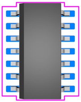
| 
| 
|
Summary of Differences
| Feature | Level A (Most) | Level B (Nominal) | Level C (Least) | | Pad Size | Largest | Medium | Smallest | | Solder Fillet | Maximum robust joint | Balanced | Minimal joint | | Ease of Rework | Easy/Rework-friendly | Moderate | Very Difficult/None | | Main Usage | High Reliability/Vibration | General Purpose | Micro-electronics (HDI) | | Acceptable Class | 1,2,3 | 1,2,3 | 1,2 |
| FOOTPRINT EXPERT GUIDELINE Topics | | https://www.pcblibraries.com/forum/terms-and-definitions_topic3672.html - Terms & Definitions https://www.pcblibraries.com/forum/component-descriptions_topic3673.html - Component Descriptions https://www.pcblibraries.com/forum/threetier-density-levels_topic3674.html - Three-Tier Density Levels | | https://www.pcblibraries.com/forum/ipc7352-mathematical-model_topic3675.html - IPC-7352 Mathematical Model Solder Joint Goal Tables: [ https://www.pcblibraries.com/forum/surface-mount-solder-joint-goal-tables-min-max_topic3676.html - Min/Max ] [ https://www.pcblibraries.com/forum/solder-joint-goal-tables-for-nominal-calculation_topic3677.html - Nominal ] | | https://www.pcblibraries.com/forum/manufacturer-recommended-patterns_topic3678.html - Manufacturer Recommended https://www.pcblibraries.com/forum/throughhole-terminals_topic3679.html - Through-hole Terminals https://www.pcblibraries.com/forum/courtyard-excess_topic3680.html - Courtyard Excess | | https://www.pcblibraries.com/forum/pcbl-footprint-naming-convention-surface-mount_topic3681.html - PCBL Footprint Convention: SM IPC-7352 Naming Convention: [ https://www.pcblibraries.com/forum/ipc7352-footprint-naming-convention-throughhole_topic3682.html - Footprint TH ] [ https://www.pcblibraries.com/forum/ipc7352-pad-stack-naming-convention_topic3685.html - Pad Stack ] | | https://www.pcblibraries.com/forum/oda-pad-stack-naming-convention_topic3686.html - ODA Pad Stack Convention https://www.pcblibraries.com/forum/terminal-lead-forms_topic3687.html - Terminal Lead Forms https://www.pcblibraries.com/forum/pad-shapes_topic3688.html - Pad Shapes https://www.pcblibraries.com/forum/design-units_topic3689.html - Design Units | | https://www.pcblibraries.com/forum/fpx-file-definition_topic3690.html - FPX File Definition https://www.pcblibraries.com/forum/smd-pad-stack-rules_topic3691.html - SMD Pad Stack Rules https://www.pcblibraries.com/forum/drafting-outlines-polarity-marking_topic3692.html - Drafting Outlines & Polarity Marking | | https://www.pcblibraries.com/forum/package-and-terminal-tolerances_topic3693.html - Package & Terminal Tolerances https://www.pcblibraries.com/forum/zero-component-orientation_topic3694.html - Zero Component Orientation | | https://www.pcblibraries.com/forum/standard-reference-designators_topic3695.html - Standard Reference Designators Component Families: [ https://www.pcblibraries.com/forum/surface-mount-component-families_topic3696.html - Surface Mount ] [ https://www.pcblibraries.com/forum/throughhole-component-families_topic3697.html - Through-hole ] |
The Footprint Expert automates footprints to perfection. Professional, detailed, and accurate parts - all built consistently with identical rules, regardless of how many people are involved in your library development.
Get your FREE Footprint Calculator or Footprint Expert Evaluation License:
https://www.pcblibraries.com/Register" target="_blank rel="nofollow" - https://www.PCBLibraries.com/Register
Call us - 847-557-2300
-------------
Stay connected - follow us! https://twitter.com/PCBLibraries" rel="nofollow - X - http://www.linkedin.com/company/pcb-libraries-inc-/" rel="nofollow - LinkedIn
|