

|
|
Surface Mount Solder Joint Goal Tables (Min / Max) |
Post Reply 
|
| Author | |
Nick B 
Admin Group 

Joined: 02 Jan 2012 Status: Offline Points: 2066 |
 Post Options Post Options
 Thanks(0) Thanks(0)
 Quote Reply Quote Reply
 Topic: Surface Mount Solder Joint Goal Tables (Min / Max) Topic: Surface Mount Solder Joint Goal Tables (Min / Max)Posted: 15 Aug 2026 at 11:00am |
|
The Min/Max Calculation section was originally inspired by IPC-7351 and subsequently by the superseding IPC-7352 – Generic Guideline for Land Pattern Design. The solder joint goals were derived from the IPC J-STD-001G - Requirements for Soldered Electrical and Electronic Assemblies. For more details, see Appendix I. Gullwing Leads (SOP, QFP, SOT, DPAK, SOD) 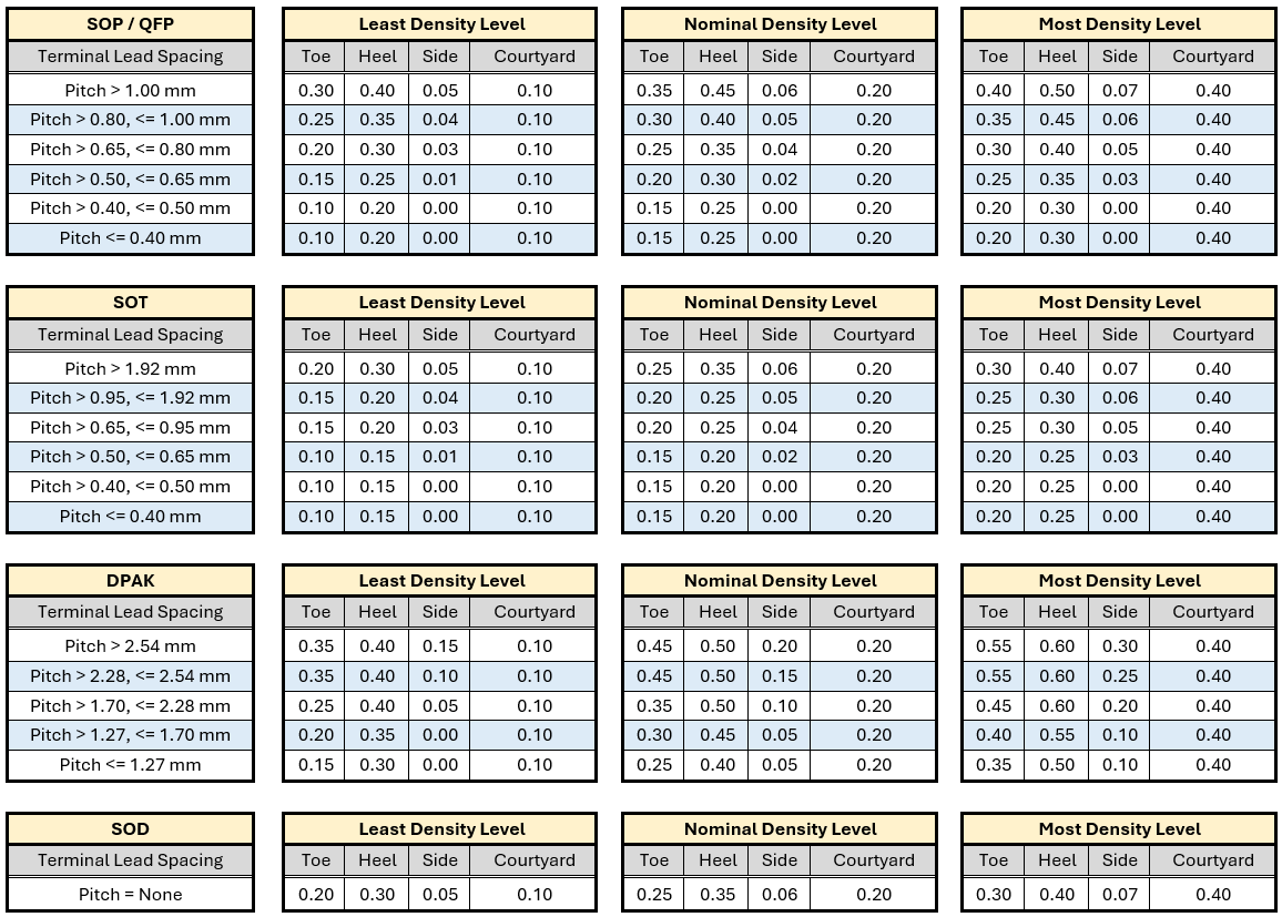 Rectangular and Square-End Cap (Chips) 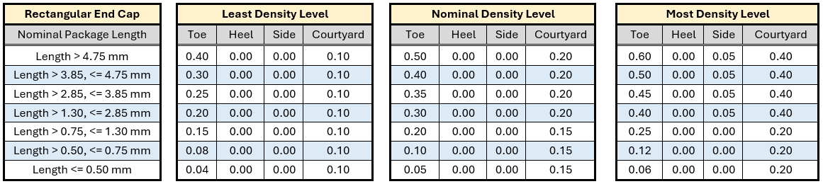 Inward L Lead Oscillator and Small Outline L-Lead (SOL)  Outward L-Lead (SOT)  Cylindrical End Cap (MELF)  Small Outline No-Lead (SON, QFN)  Small Outline Components, Flat Lead (SOFL, SODFL)  Flat Lug Lead (DPAK)  Small Outline Flat No-Lead Bottom (DFN, LGA, PSON, PQFN)  Under-Body Outward L-Lead (Aluminum Electrolytic Capacitor, Crystal)  Inward Flat Ribbon L-Lead (Molded Body)  Concave & Convex Chip Array and Leadless Chip Carrier (LCC) 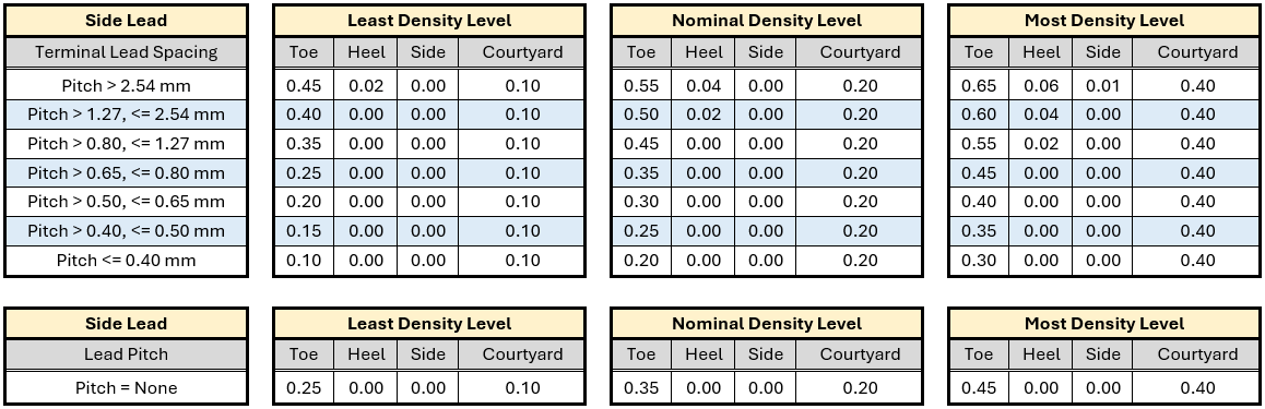 J-Leads  Column and Land Grid Array (CGA & LGA)  Corner Concave Oscillator  Collapsing and Non-Collapsing Ball Grid Array (BGA) 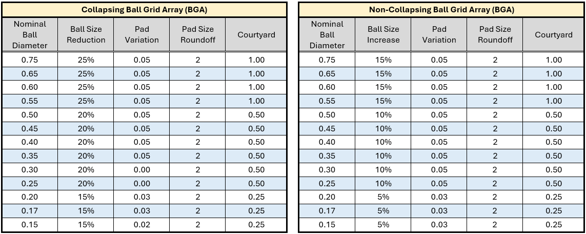 |
|
 |
|

|
|
|
|
|
Post Reply
|
|
| Tweet |
| Forum Jump | Forum Permissions You cannot post new topics in this forum You cannot reply to topics in this forum You cannot delete your posts in this forum You cannot edit your posts in this forum You cannot create polls in this forum You cannot vote in polls in this forum |


 Topic Options