
|
|
DPAK and SOT-89 Can be a bit tricky... |
Post Reply 
|
| Author | ||
Nick B 
Admin Group 

Joined: 02 Jan 2012 Status: Offline Points: 2096 |
 Post Options Post Options
 Thanks(0) Thanks(0)
 Quote Reply Quote Reply
 Topic: DPAK and SOT-89 Can be a bit tricky... Topic: DPAK and SOT-89 Can be a bit tricky...Posted: 9 hours 11 minutes ago at 9:38pm |
|
ANSWER: The part on POD has the manufacturer recommended pattern. 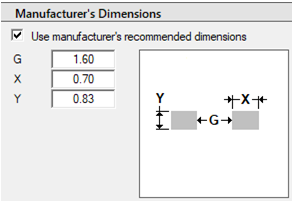 When you recalculate, the manufacturer recommended pattern resets to the default IPC rules. You need to reinsert the mfr. recommended pattern dimensions.
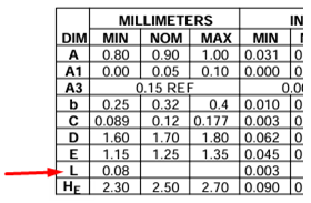
ANSWER: If the component manufacturer only provides a Minimum 'L' dimension, using the manufacturer recommended pattern solves the missing Maximum value. Also, Diodes may carry high voltage current, and the manufacturer wants to enlarge the pads to carry the current. Same with DPAK voltage regulators - they carry high current and it may be wise to use their recommended pattern. You're on the right track. |
||
 |
||

|
||
|
||
|
Post Reply
|
|
| Tweet |
| Forum Jump | Forum Permissions You cannot post new topics in this forum You cannot reply to topics in this forum You cannot delete your posts in this forum You cannot edit your posts in this forum You cannot create polls in this forum You cannot vote in polls in this forum |


 Topic Options