DPAK and SOT-89 Can be a bit tricky...
Printed From: PCB Libraries Forum
Category: PCB Footprint Expert
Forum Name: Questions & Answers
Forum Description: issues and technical support
URL: https://www.PCBLibraries.com/forum/forum_posts.asp?TID=3702
Printed Date: 02 Sep 2026 at 7:17am
Topic: DPAK and SOT-89 Can be a bit tricky...
Posted By: Nick B
Subject: DPAK and SOT-89 Can be a bit tricky...
Date Posted: 01 Sep 2026 at 9:38pm
ANSWER: The part on POD has the manufacturer recommended pattern. 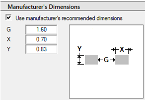 When you recalculate, the manufacturer recommended pattern resets to the default IPC rules. You need to reinsert the mfr. recommended pattern dimensions.
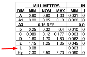
ANSWER: If the component manufacturer only provides a Minimum 'L' dimension, using the manufacturer recommended pattern solves the missing Maximum value. Also, Diodes may carry high voltage current, and the manufacturer wants to enlarge the pads to carry the current. Same with DPAK voltage regulators - they carry high current and it may be wise to use their recommended pattern. You're on the right track. ------------- Stay connected - follow us! https://twitter.com/PCBLibraries" rel="nofollow - X - http://www.linkedin.com/company/pcb-libraries-inc-/" rel="nofollow - LinkedIn |