

|
|
Why is Gang Mask shape option removed? |
Post Reply 
|
Page <12 |
| Author | |
Tom H 
Admin Group 

Joined: 05 Jan 2012 Location: San Diego, CA Status: Offline Points: 6096 |
 Post Options Post Options
 Thanks(0) Thanks(0)
 Quote Reply Quote Reply
 Posted: 06 Jan 2025 at 1:59pm Posted: 06 Jan 2025 at 1:59pm |
|
Altium has it's own Preferences for solder mask control. Regardless of any setting you establish in Footprint Expert Options, Altium Preferences will overwrite the Footprint Expert settings.
The disable the gang mask feature, make your solder mask swell 0.00 (or 1:1 scale of the pad stack). When you import the footprint into Altium, the Altium Preferences will take over. You need to do the math to establish a solder mask sliver between every pad stack. Start with the minimum solder mask sliver size of 0.075. Then add the solder mask swell of 0.05. The minimum pad to pad spacing rule needs to be set for 0.175 for pad trimming. Only the pads for a 0.50 pin pitch will need to be trimmed. |
|
 |
|

|
|
|
|
|
ulissescastro
Active User 
Joined: 23 Feb 2022 Status: Offline Points: 18 |
Post Options
Thanks(1)
Quote Reply
Posted: 06 Jan 2025 at 1:31pm |
|
Hi Tom, I'm having some trouble understanding how to disable the Gang feature and control it as needed. The only guidance I found is a comment saying, "set sm grid array options in terminal density settings" in the SMD Pad Stack Rules. I can manage the solder mask web using mask expansions and pad-to-pad settings to ensure the minimum web. However, I want to be able to enable or disable this control. Our assembly house prefers to have a mask between pads to minimize the risk of solder bridging and to allow more width for the stencil apertures. Therefore, I would rather trim the leads, knowing exactly what I'm doing |
|
|
|
|
Tom H
Admin Group
Joined: 05 Jan 2012 Location: San Diego, CA Status: Offline Points: 6096 |
Post Options
Thanks(1)
Quote Reply
Posted: 06 Jan 2025 at 11:33am |
|
Other V25.02 improvements to the Altium interface:
|
|
|
|
|
Tom H
Admin Group
Joined: 05 Jan 2012 Location: San Diego, CA Status: Offline Points: 6096 |
Post Options
Thanks(1)
Quote Reply
Posted: 06 Jan 2025 at 11:27am |
|
The Gang Mask shape is now determined by the pad shape.
Rectangle pad shape will automatically produce a rectangle gang mask. Rounded Rectangle pad shape will automatically produce a rounded rectangle gang mask. Oblong pad shape will automatically produce an oblong gang mask. The V25.02 Footprint Expert gang mask feature has been updated and improved. The gang mask feature will appear in the Footprint Expert viewer. 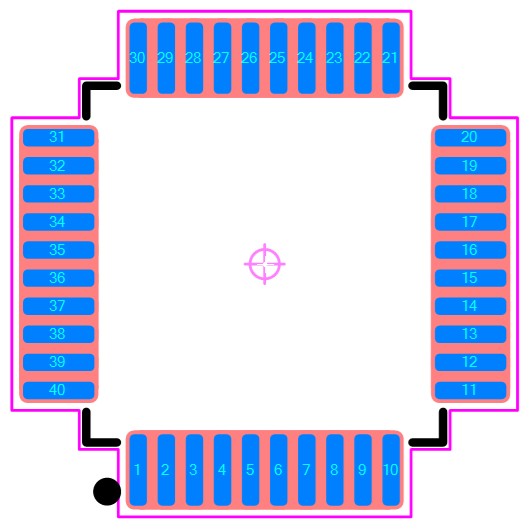 |
|
|
|
|
ulissescastro
Active User
Joined: 23 Feb 2022 Status: Offline Points: 18 |
Post Options
Thanks(1)
Quote Reply
Posted: 06 Jan 2025 at 11:13am |
|
Hi Tom, Could you please elaborate on why the Gang Mask option was removed in the latest version? I also noticed that FPE does not visually show the "block" until it is imported into Altium (in my case). Adding individual "lines" to construct the "block" in the solder mask layer may not be efficient when the user wants to delete it. Could you please create a shape that can be easily removed with a single selection? Best regards, |
|
|
|
|
Post Reply
|
Page <12 |
| Tweet |
| Forum Jump | Forum Permissions You cannot post new topics in this forum You cannot reply to topics in this forum You cannot delete your posts in this forum You cannot edit your posts in this forum You cannot create polls in this forum You cannot vote in polls in this forum |


 Topic Options