

|
|
IPC-7351 Padstack Naming Convention |
Post Reply 
|
Page 123 4> |
| Author | |
Tom H 
Admin Group 

Joined: 05 Jan 2012 Location: San Diego, CA Status: Offline Points: 6033 |
 Post Options Post Options
") Thanks(1) Thanks(1)
 Quote Reply Quote Reply
 Topic: IPC-7351 Padstack Naming Convention Topic: IPC-7351 Padstack Naming ConventionPosted: 07 Apr 2024 at 2:30pm |
|
Updated Pad Stack Naming Convention released in IPC-7352. 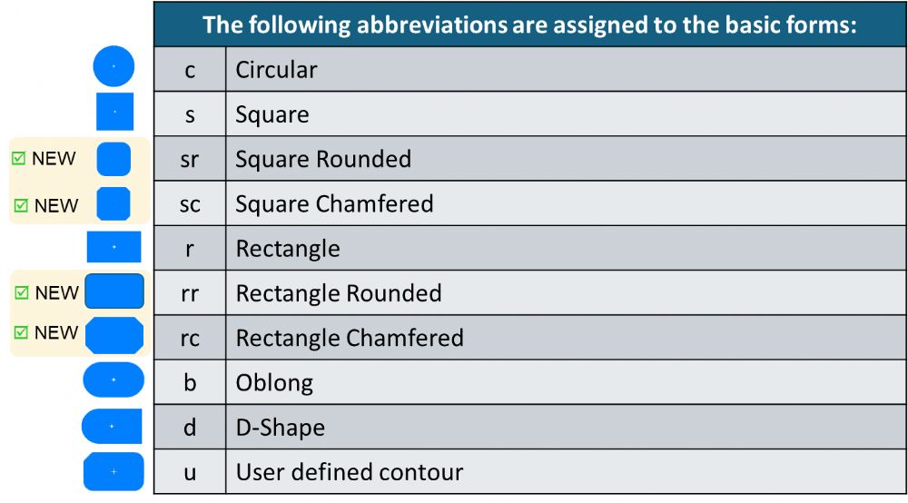 |
|
 |
|

|
|
|
|
|
AleksMK
New User 
Joined: 31 Mar 2020 Status: Offline Points: 4 |
Post Options
Thanks(0)
Quote Reply
Posted: 29 Apr 2020 at 10:43am |
|
Thanks! So I will name my padstack xc120mx130px0. Cheers! Aleks
|
|
|
|
|
Tom H
Admin Group
Joined: 05 Jan 2012 Location: San Diego, CA Status: Offline Points: 6033 |
Post Options
Thanks(1)
Quote Reply
Posted: 29 Apr 2020 at 10:08am |
|
Modifiers that are used when pad stack features are different than the defaults x = Special modifier
used alone or following other modifiers for lands on opposite side to primary
layer land dimension So the "x" comes before the shape character. |
|
|
|
|
AleksMK
New User
Joined: 31 Mar 2020 Status: Offline Points: 4 |
Post Options
Thanks(0)
Quote Reply
Posted: 29 Apr 2020 at 9:44am |
|
Hi Tom, Thanks for all the info, although a bit unrelated to my question :-) The application for which I need this padstack is creating test points in OrCAD PCB Designer Professional, where the padstack need to be defined on the layer where you are creating the test point. So if I want a test point on the bottom layer, I need to have the bottom layer defined in my padstack. The padstack is not being mirrored when adding testpoints, hence this requirement. If I may re-iterate my question: using the padstack naming convention that I have downloaded from PCB Libraries, what is the correct name to name a padstack which will have a circular land patter on the bottom layer only 1.2mm in
size, with a solder mask on the bottom layer only with 1.3mm opening
and no bottom paste mask layer? Cheers
|
|
|
|
|
Tom H
Admin Group
Joined: 05 Jan 2012 Location: San Diego, CA Status: Offline Points: 6033 |
Post Options
Thanks(0)
Quote Reply
Posted: 29 Apr 2020 at 9:34am |
|
There is a pad stack naming issue with the current V2019 Library Expert for SMD pads that are defined on both the Top and Bottom layers. This issue will be fixed in V2020 coming out next month.
To create a complex pad stack, you need the FP Designer feature and that does not come with the free Library Expert Pro (yet), but next month when V2020 is released, the Library Expert Pro will have 100% full featured program (just like the Enterprise version) and support these CAD tools -
Also, starting next week we start giving away the full featured Library Expert Enterprise for free. Just pay the yearly maintenance to get all the updates and technical support for the year. Pick any CAD tool and get our new Cloud License for a yearly lease at 20% of list price. Bottom line is that you need FP Designer to create custom pad stacks and we're either going to give that away for free or lease it at an affordable price point. The software program needs to work perfect to take away any guessing and confusion. Also, putting a SMD pad on the top & bottom layers is rare. What application is this for? |
|
|
|
|
AleksMK
New User
Joined: 31 Mar 2020 Status: Offline Points: 4 |
Post Options
Thanks(0)
Quote Reply
Posted: 29 Apr 2020 at 7:56am |
|
Hi Tom, Yes, I do have the document, the question arose from reading that document. As I quoted, It's not very clear to me how the naming for my padstack should be? Any advice on that? Thanks! Aleks
|
|
|
|
|
Tom H
Admin Group
Joined: 05 Jan 2012 Location: San Diego, CA Status: Offline Points: 6033 |
Post Options
Thanks(0)
Quote Reply
Posted: 29 Apr 2020 at 7:31am |
|
AleksMK, do you have a copy of the pad stack naming convention document?
You can download it here - www.pcblibraries.com/downloads |
|
|
|
|
AleksMK
New User
Joined: 31 Mar 2020 Status: Offline Points: 4 |
Post Options
Thanks(0)
Quote Reply
Posted: 29 Apr 2020 at 6:50am |
|
Hi everyone, I have a question on the use of the special x modifier. This is it's definition: "x = Special modifier
used alone or following other modifiers for lands on opposite side to primary
layer land dimension" And later on there are three examples: mxc = Solder Mask
Opposite Side Circular
mx0 = Solder Mask Opposite Side No Solder Mask xc = Opposite Side Circular As the x-modifier is defined that it is following other modifier, is the last "xc" example wrong? Should it not be "cx"? I need to create a padstack, which will have a circular land patter on the bottom layer only 1.2mm in size, with a solder mask on the bottom layer only with 1.3mm opening and no bottom paste mask layer. Which of the following namings (or none?) will be the correct one for this padstack? 1. cx120mx130px0 2. xc120mx130px0 3. xc120xm130xp0 Thanks! Aleks |
|
|
|
|
jameshead
Expert User 

Joined: 20 Mar 2012 Location: Oxfordshire, UK Status: Offline Points: 576 |
Post Options
Thanks(0)
Quote Reply
Posted: 05 Oct 2015 at 5:45am |
|
Another example of padstyle of the top "layer 1" may be different to the inner and bottom layers is a TO-220 horizontal where you have a rectangular pad to connect with the heatsink of the device and have only a round pad on inner and the bottom layer.
I've interpreted the standard to have: r1599_1039r25o510xc580zc580h385 Rectangular 15.99 mm x 10.39 mm, radius 0.25 mm corners for a pad on layer 1, where the centre of the rectangular pad is off-set 5.1 mm from the centre of the hole. Hole size is 3.85 mm. Pads on inner layers and the bottom size is a round 5.80 mm. Not all CAD systems allow you do this easily though. |
|
|
|
|
Matthew Lamkin
Advanced User 
Joined: 02 Oct 2012 Status: Offline Points: 284 |
Post Options
Thanks(0)
Quote Reply
Posted: 05 Oct 2015 at 4:39am |
 Cheers Tom. |
|
|
|
|
Post Reply
|
Page 123 4> |
| Tweet |
| Forum Jump | Forum Permissions You cannot post new topics in this forum You cannot reply to topics in this forum You cannot delete your posts in this forum You cannot edit your posts in this forum You cannot create polls in this forum You cannot vote in polls in this forum |


 Topic Options