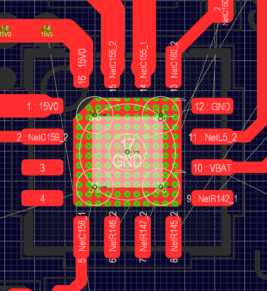
Small Pad with Larger Copper Shape
Printed From: PCB Libraries Forum
Category: PCB Footprint Expert
Forum Name: Questions & Answers
Forum Description: issues and technical support
URL: https://www.PCBLibraries.com/forum/forum_posts.asp?TID=3708
Printed Date: 12 Oct 2026 at 11:45am
Topic: Small Pad with Larger Copper Shape
Posted By: Nick B
Subject: Small Pad with Larger Copper Shape
Date Posted: 12 Oct 2026 at 8:44am
ANSWER: The answer is simple. Chamfered Thermal Pads in a corner by Pin 1 are not 'Flash' apertures. They are Copper Polygon Shapes and are drawn and not flashed. To make a thermal pad a Flash Aperture (a normal pad), remove the corner chamfer. ------------- Stay connected - follow us! https://twitter.com/PCBLibraries" rel="nofollow - X - http://www.linkedin.com/company/pcb-libraries-inc-/" rel="nofollow - LinkedIn |