|
The IPC-7352 standard defines the mathematical model for creating reliable surface mount (SMD) PCB footprints by providing formulas to calculate pad width (X), pad spacing (G), and pad span (Z), based on component dimensions, solder fillet goals, and manufacturing tolerances.
The following images illustrate potential pad and terminal relationships under various Material Conditions - Minimum, Nominal, and Maximum.
- The Nominal Material condition of the component package & Nominal Terminal.
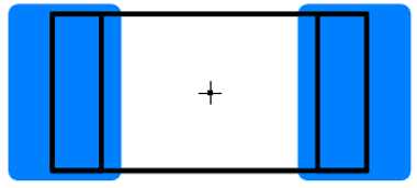 - The Minimum Material condition of the component package & Nominal Terminal.
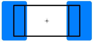 - The Maximum Material condition of the component package & Nominal Terminal.
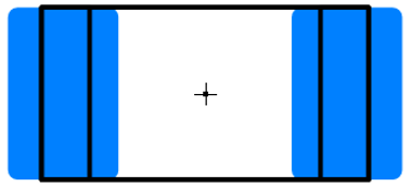 - The Minimum Material condition of the component package & Minimum Terminal.
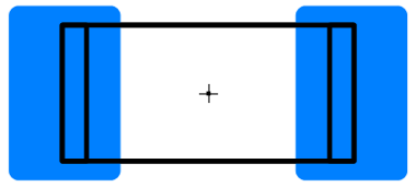 - The Maximum Material condition of the component package & Maximum Terminal.
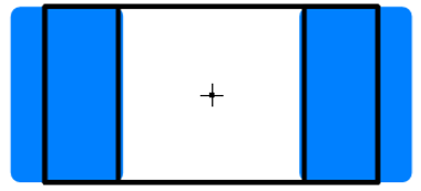
The resulting pad stack must have terminal leads on the pad stack regardless of every possible Material Condition possible to pass assembly inspection and meet the requirements set forth in the IPC J-STD-001 Standard and the IPC-7352 Guideline.
i.e.: regardless of the Component Package and Terminal Lead Material Condition, the Terminal Lead must never be exposed outside the calculated pad stack.
Note: most component packages are created in the Nominal Material Conditions. The package tolerances play a key role in the resulting pad stack.
- Nominal Package Dimensions & no Package Tolerances.

The Footprint Expert uses the IPC-7352 Mathematical Model. For details, see https://shop.ipc.org/ipc-7352/ipc-7352-standard-only/Revision-0/english - IPC-7352 .
| FOOTPRINT EXPERT GUIDELINE Topics | | https://www.pcblibraries.com/forum/terms-and-definitions_topic3672.html - Terms & Definitions https://www.pcblibraries.com/forum/component-descriptions_topic3673.html - Component Descriptions https://www.pcblibraries.com/forum/threetier-density-levels_topic3674.html - Three-Tier Density Levels | | https://www.pcblibraries.com/forum/ipc7352-mathematical-model_topic3675.html - IPC-7352 Mathematical Model Solder Joint Goal Tables: [ https://www.pcblibraries.com/forum/surface-mount-solder-joint-goal-tables-min-max_topic3676.html - Min/Max ] [ https://www.pcblibraries.com/forum/solder-joint-goal-tables-for-nominal-calculation_topic3677.html - Nominal ] | | https://www.pcblibraries.com/forum/manufacturer-recommended-patterns_topic3678.html - Manufacturer Recommended https://www.pcblibraries.com/forum/throughhole-terminals_topic3679.html - Through-hole Terminals https://www.pcblibraries.com/forum/courtyard-excess_topic3680.html - Courtyard Excess | | https://www.pcblibraries.com/forum/pcbl-footprint-naming-convention-surface-mount_topic3681.html - PCBL Footprint Convention: SM IPC-7352 Naming Convention: [ https://www.pcblibraries.com/forum/ipc7352-footprint-naming-convention-throughhole_topic3682.html - Footprint TH ] [ https://www.pcblibraries.com/forum/ipc7352-pad-stack-naming-convention_topic3685.html - Pad Stack ] | | https://www.pcblibraries.com/forum/oda-pad-stack-naming-convention_topic3686.html - ODA Pad Stack Convention https://www.pcblibraries.com/forum/terminal-lead-forms_topic3687.html - Terminal Lead Forms https://www.pcblibraries.com/forum/pad-shapes_topic3688.html - Pad Shapes https://www.pcblibraries.com/forum/design-units_topic3689.html - Design Units | | https://www.pcblibraries.com/forum/fpx-file-definition_topic3690.html - FPX File Definition https://www.pcblibraries.com/forum/smd-pad-stack-rules_topic3691.html - SMD Pad Stack Rules https://www.pcblibraries.com/forum/drafting-outlines-polarity-marking_topic3692.html - Drafting Outlines & Polarity Marking | | https://www.pcblibraries.com/forum/package-and-terminal-tolerances_topic3693.html - Package & Terminal Tolerances https://www.pcblibraries.com/forum/zero-component-orientation_topic3694.html - Zero Component Orientation | | https://www.pcblibraries.com/forum/standard-reference-designators_topic3695.html - Standard Reference Designators Component Families: [ https://www.pcblibraries.com/forum/surface-mount-component-families_topic3696.html - Surface Mount ] [ https://www.pcblibraries.com/forum/throughhole-component-families_topic3697.html - Through-hole ] |
The Footprint Expert automates footprints to perfection. Professional, detailed, and accurate parts - all built consistently with identical rules, regardless of how many people are involved in your library development.
Get your FREE Footprint Calculator or Footprint Expert Evaluation License:
https://www.pcblibraries.com/Register" target="_blank rel="nofollow" - https://www.PCBLibraries.com/Register
Call us - 847-557-2300
-------------
Stay connected - follow us! https://twitter.com/PCBLibraries" rel="nofollow - X - http://www.linkedin.com/company/pcb-libraries-inc-/" rel="nofollow - LinkedIn
|