IPC-735x Evolutions
Printed From: PCB Libraries Forum
Category: Libraries
Forum Name: Footprints / Land Patterns
Forum Description: [General or a CAD specific issues / discussions]
URL: https://www.PCBLibraries.com/forum/forum_posts.asp?TID=3576
Printed Date: 26 Jul 2026 at 3:21pm
Topic: IPC-735x Evolutions
Posted By: sot23
Subject: IPC-735x Evolutions
Date Posted: 18 Nov 2025 at 8:23am
|
Hello, my team recently purchased the IPC-7352 released in 2023 and I am currently in the process of studying it to decide whether we should make it our new standard for footprints creation or not. For the moment I must admit that I am not thrilled by what I have read. Some exemples :
My question : what do you all think about 7352 ? I would be very interested in your opinion specifically, Tom H, as I know you are very much involved in the IPC talks (thanks for all your work on that by the way). Is it a good upgrade to 7351B ? Honestly I was hoping for more. But maybe I am a bit to difficult... Sorry if my English is not perfect, as it is not my primary language.
|
Replies:
Posted By: Tom H
Date Posted: 18 Nov 2025 at 8:56am
|
IPC-7351B and IPC-7352 are identical for Surface Mount. No change except the pad stack naming convention added a double 'rr' for Rounded Rectangle pad shape. IPC-7352 introduced Through-hole technology, but most of the information was extracted from IPC-2221 & IPC-2222. The main thing that was added was the Through-hole land pattern naming convention which we created in 2008 but shelved until 2023. The IPC-735x series misses the mark in several areas. - Solder joint goals 'one size fits all' doesn't produce the best assembly attachment and it doesn't adhere to IPC J-STD-001. Also, the values between density levels is too robust. Most is too Most and Least is too Least. - The naming convention puts the 'pin qty' at the end of the footprint name. This was changed in the IPC-7351C standard that was unanimously approved by the land pattern committee but never got released. - The Zero Component Rotation differs from the standard they replaced - IPC-SM-782 Related posts: https://www.pcblibraries.com/forum/ipc7352-vs-pcb-libraries-footprint-naming-option_topic3488_post13869.html?KW=IPC%2D7352#13869" rel="nofollow - https://www.pcblibraries.com/forum/ipc7352-vs-pcb-libraries-footprint-naming-option_topic3488_post13869.html?KW=IPC%2D7352#13869 https://www.pcblibraries.com/forum/pcb-pad-footprint-orientation_topic3460_post14010.html?KW=IPC%2D7351B#14010" rel="nofollow - https://www.pcblibraries.com/forum/pcb-pad-footprint-orientation_topic3460_post14010.html?KW=IPC%2D7351B#14010 ------------- Stay connected - follow us! https://twitter.com/PCBLibraries" rel="nofollow - X - http://www.linkedin.com/company/pcb-libraries-inc-/" rel="nofollow - LinkedIn |
Posted By: sot23
Date Posted: 19 Nov 2025 at 9:05am
|
Thank your for the answer. "IPC-7351B and IPC-7352 are identical for Surface Mount. No change except the pad stack naming convention added a double 'rr' for Rounded Rectangle pad shape." That is not what I see when I read both documents side by side : Table 3-3 (page 10) of the 7352 specify a Toe calculation for Square ends components with W=<0.5mm that, on the Median footprint, is dependent of the height of the component (which I think totally makes sense when comparing to J-STD-001). This is not the case for the 7351 (table 3-5, page 17). As this height dependency is only for the N footprint, it leads to cases where the N pads are smaller than the L pads, which seems strange. "IPC-7352 introduced Through-hole technology, but most of the information was extracted from IPC-2221 & IPC-2222." The Through hole calculation (4.4.1, table 4-1 and 4-2) is in direct contradiction to the calculation in IPC 2222 (Table 9-5). Or I am having big trouble understanding theses tables. Theses are mostly the points that confuses me. Thank you for the linked posts. It is very interesting to know the history behind these standards.
|
Posted By: Tom H
Date Posted: 19 Nov 2025 at 10:16am
|
The unreleased IPC-7351C had new solder joint goal tables for Gull Wing and Rectangular or Square End Cap packages. The Square End Cap solder joint goals need to have unique Toe values for every chip size. 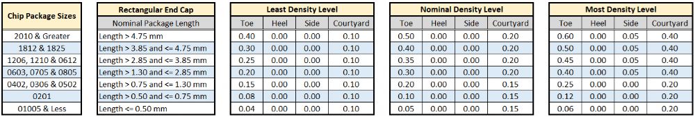 The Gullwing terminal lead needs a different toe goal for every pin pitch. 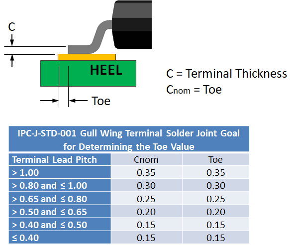 SOP/QFP Table: 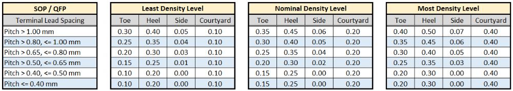 ------------- Stay connected - follow us! https://twitter.com/PCBLibraries" rel="nofollow - X - http://www.linkedin.com/company/pcb-libraries-inc-/" rel="nofollow - LinkedIn |