Map Assembly & Silkscreen Outline to L x W Maximum
Printed From: PCB Libraries Forum
Category: PCB Footprint Expert
Forum Name: Questions & Answers
Forum Description: issues and technical support
URL: https://www.PCBLibraries.com/forum/forum_posts.asp?TID=3564
Printed Date: 18 Jun 2026 at 3:23am
Topic: Map Assembly & Silkscreen Outline to L x W Maximum
Posted By: m.elsayed
Subject: Map Assembly & Silkscreen Outline to L x W Maximum
Date Posted: 21 Oct 2025 at 4:48am
When using Footprint Expert, and align with below parameters to achieve "Outline of the component body (Length X Width) with max. dimensions with 0.127 mm line width.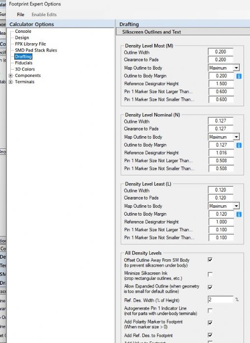 However the resulting values are larger than max values like values should be 3*1.4 but appears in Altium as 3.128*1.528. Attached FPX file - uploads/11979/silkscreen_dimenstion.fpx" rel="nofollow - uploads/11979/silkscreen_dimenstion.fpx 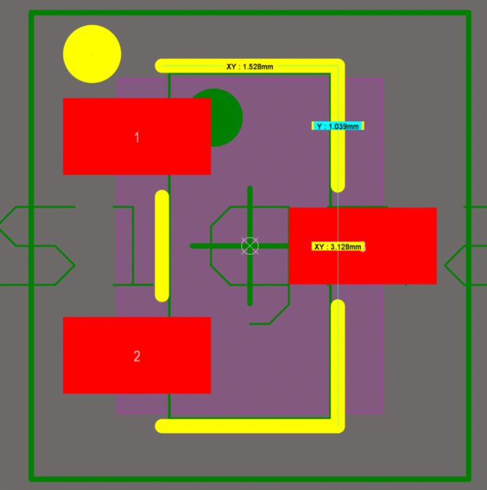 |
Replies:
Posted By: Tom H
Date Posted: 21 Oct 2025 at 8:38am
|
It's because you have the 'Offset Outline Away From SM Body' selected. Unselect this Option and remeasure. 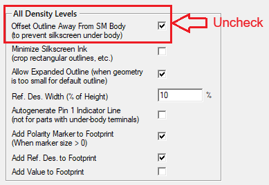 This is only for Surface Mount Silkscreen Outlines. ------------- Stay connected - follow us! https://twitter.com/PCBLibraries" rel="nofollow - X - http://www.linkedin.com/company/pcb-libraries-inc-/" rel="nofollow - LinkedIn |
Posted By: m.elsayed
Date Posted: 21 Oct 2025 at 9:00am
| can please give more details about this feature ? |
Posted By: Tom H
Date Posted: 21 Oct 2025 at 9:07am
|
You can test is locally in the Calculator Options by checking and unchecking the Silkscreen Drafting Options? The 'origin' of the line is the centerline when unchecked. The 'origin' of the line is the inside line edge when checked. ------------- Stay connected - follow us! https://twitter.com/PCBLibraries" rel="nofollow - X - http://www.linkedin.com/company/pcb-libraries-inc-/" rel="nofollow - LinkedIn |
Posted By: m.elsayed
Date Posted: 21 Oct 2025 at 9:26am
|
Can you add an image that illustrates this Offset Line description and how it affects the Altium dimensions? |
Posted By: Tom H
Date Posted: 21 Oct 2025 at 9:51am
|
Silkscreen Line with No Offset. 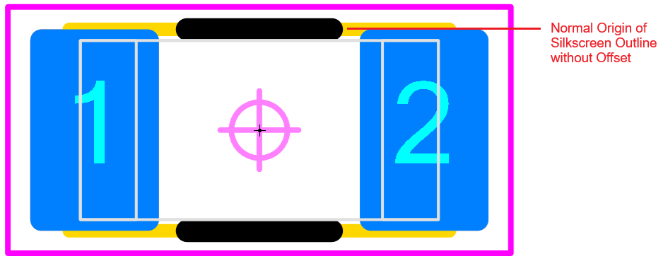 Silkscreen Line with Offset. 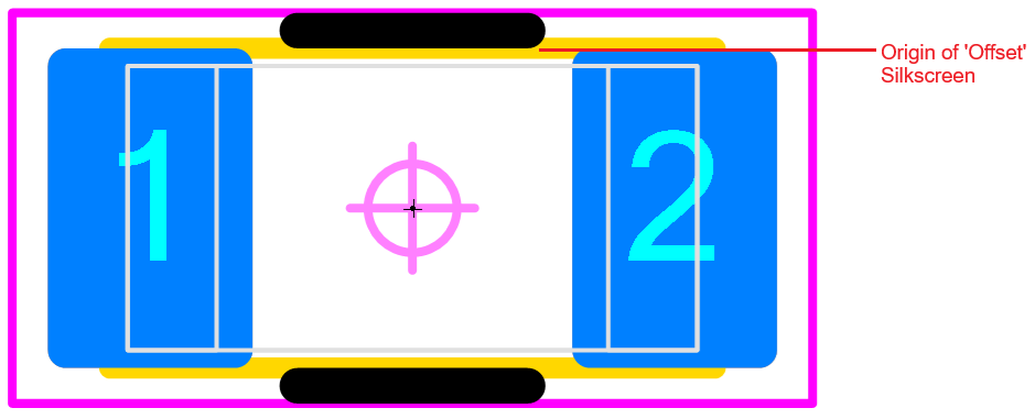 ------------- Stay connected - follow us! https://twitter.com/PCBLibraries" rel="nofollow - X - http://www.linkedin.com/company/pcb-libraries-inc-/" rel="nofollow - LinkedIn |
Posted By: m.elsayed
Date Posted: 21 Oct 2025 at 10:06am
|
I think there is no big difference am I correct? Also is this option checked will cause issue on design? What you think to apply requirement “component body outline Lxw with max diemsion Check option or not check? |
Posted By: Tom H
Date Posted: 21 Oct 2025 at 10:20am
|
Silkscreen on solder mask creates a small bump. This is why silkscreen under the package body (especially very small low profile packages) is unacceptable because it can lift the package up just enough to cause solder joint problems. Due to the IPC J-STD-001 and the slop tolerance component package positioning that is allowed for assembly acceptability, using the no silkscreen offset can cause soldering problems if the component package moves over the silkscreen during reflow. When you Offset the silkscreen outline, it kind of compensates for the package movement (tolerance) during reflow. Especially when you map the silkscreen to the Maximum Body Dimension. However, some assembly shops with a higher level of component package movement during reflow, will use the Offset Margin Option to move the silkscreen further away from the package body. It depends on the assembly shop quality and accuracy. Some shops use older equipment and require robust tolerances. While some assembly shops use new equipment with very high placement accuracy levels. Talk to your assembly shop and ask them what there placement tolerances are. ------------- Stay connected - follow us! https://twitter.com/PCBLibraries" rel="nofollow - X - http://www.linkedin.com/company/pcb-libraries-inc-/" rel="nofollow - LinkedIn |