Solder and Paste Mask Expansion
Printed From: PCB Libraries Forum
Category: PCB Footprint Expert
Forum Name: Questions & Answers
Forum Description: issues and technical support
URL: https://www.PCBLibraries.com/forum/forum_posts.asp?TID=3536
Printed Date: 25 Jun 2026 at 5:21am
Topic: Solder and Paste Mask Expansion
Posted By: m.elsayed
Subject: Solder and Paste Mask Expansion
Date Posted: 13 Sep 2025 at 12:01pm
|
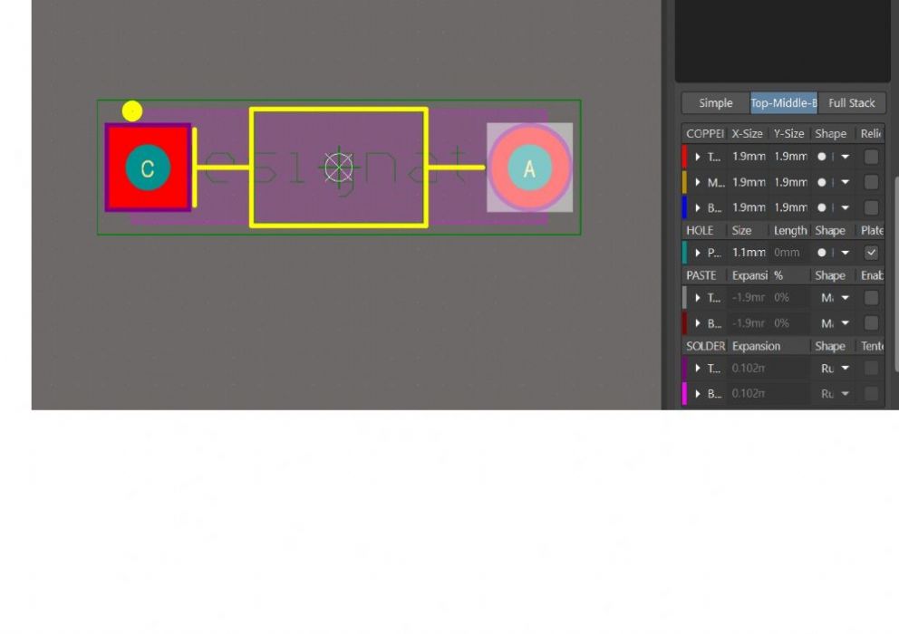
I set my Master Option settings for SMD solder and paste mask expansion to zero '0'. I use the Altium translator I unselect 'Use Altium Mask Expansion Rules'. When I open the footprint in Altium, the Paste Mask value is zero. Especially through-hole footprints. How do I solve this? |
Replies:
Posted By: Tom H
Date Posted: 13 Sep 2025 at 1:13pm
|
The Altium translator command 'Use Altium Mask Expansion Rules' is intended for Solder Mask (not Paste Mask). The Paste Mask default setting is 0.00. This produces a 1:1 scale paste mask per the SMD pad. You can use positive and negative values to expand or reduce paste mask aperture. There is also a settings for adjusting the paste mask by a percentage value. Footprint Expert has multiple settings for Solder Mask Expansion in the Option file.
Setting the Solder Mask Expansion value to 0.00 will make the solder mask 1:1 scale of the pad stack. This allows the fabrication shop to swell the solder mask to a value that supports their solder mask application tolerances. Altium has internal 'Preferences' that allows the user to set to global solder mask swell. Altium has DRC rules for checking Silkscreen on Solder Mask. You don't want Silkscreen Reference Designators on Solder Mask. If you place a Ref Des on Solder Mask, the fabrication CAM Operator will trim it and that could make the ref des illegible. That's why Altium has a DRC for checking and reporting silkscreen to solder mask violations. The Footprint Expert Altium translator option for 'Use Altium Mask Expansion Rules' is checked on by default. This ignores the Footprint Expert solder mask settings and uses the Altium 'Preferences' solder mask rules. If you uncheck 'Use Altium Mask Expansion Rules' in the Footprint Expert Altium translator, Altium will use the Footprint Expert solder mask rules and ignore the Altium 'Preferences'. If the solder mask swell is 1:1 scale in Altium, then the DRC rule for checking ref des on solder mask will be disabled and every ref des that violates the fabrication shop solder mask expansion will be trimmed by the PCB CAM operator. I don't think you want 1:1 scale solder mask in Altium. ------------- Stay connected - follow us! https://twitter.com/PCBLibraries" rel="nofollow - X - http://www.linkedin.com/company/pcb-libraries-inc-/" rel="nofollow - LinkedIn |
Posted By: Tom H
Date Posted: 13 Sep 2025 at 1:16pm
|
I don't know what you are referring to - Paste Mask on Through-hole pad stacks? Are you using 'Pin-in-Paste' technology? Or are you referring to Solder Mask on Through-hole pad stacks? You set this in 'Tools > Options > Terminals > Through-hole > Solder Mask'. ------------- Stay connected - follow us! https://twitter.com/PCBLibraries" rel="nofollow - X - http://www.linkedin.com/company/pcb-libraries-inc-/" rel="nofollow - LinkedIn |
Posted By: m.elsayed
Date Posted: 14 Sep 2025 at 2:29am
|
Thanks for your reply,however i have adjusted all of these but when open in altium 1-result not 0
2- pad has type not simple
|
Posted By: m.elsayed
Date Posted: 14 Sep 2025 at 2:29am
|
Posted By: m.elsayed
Date Posted: 14 Sep 2025 at 2:11pm
| can please support on this case |