|
|
IPC-7351 SMD & PTH Reference Calculators |
Post Reply 
|
Page 123> |
| Author | |
Nick B 
Admin Group 

Joined: 02 Jan 2012 Status: Offline Points: 1994 |
 Post Options Post Options
") Thanks(0) Thanks(0)
 Quote Reply Quote Reply
 Topic: IPC-7351 SMD & PTH Reference Calculators Topic: IPC-7351 SMD & PTH Reference CalculatorsPosted: 07 Jan 2013 at 2:35pm |
|
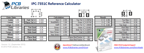
Here are the latest Reference Calculators. Please note there are TWO (2), one is Surface Mount, and the other Plated Through Hole, also referred to as TH. (you need to be logged in, registration is absolutely free!) IPC-7351 SMD Reference Calculator Below is the is the PCB Library Expert PTH Reference Calculator: 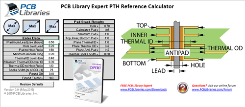 |
|
 |
|

|
|
|
|
|
jk-999
New User 

Joined: 12 Dec 2012 Status: Offline Points: 1 |
Post Options
Thanks(0)
Quote Reply
Posted: 02 Apr 2014 at 9:00am |
|
Which equation is correct? Zmax=Lmin +2JT + SQRT((CL)² + (2*F)² + (2*P)²) or
Zmax=Lmin +2JT + SQRT((CL)² + (F)² + (P)²)
IPC 7351A uses the second equation. I believe the calculator is using the first equation.
|
|
|
|
|
Jeff.M
Admin Group
Joined: 16 May 2012 Location: San Diego Status: Offline Points: 500 |
Post Options
Thanks(0)
Quote Reply
Posted: 02 Apr 2014 at 12:44pm |
|
Both are correct. The difference is due to the definitions of the 'Placement' (P) and 'Fabrication' (F) tolerances. IPC-7351 demonstrates them as a single value. For example in their publication they use 0.10 mm for F and 0.20 mm for P (this is your 2nd equation). We use plus-or-minus values where an equivalent F would be +/- 0.05 mm and P would be +/- 0.10 mm so they're doubled before squaring (this is your 1st equation). Either way, the tolerances are the same and the result is the same.
|
|
|
|
|
Nick B
Admin Group
Joined: 02 Jan 2012 Status: Offline Points: 1994 |
Post Options
Thanks(0)
Quote Reply
Posted: 20 Oct 2014 at 12:53pm |
|
Please note the IPC-7351 Reference Calculator was just updated! There is now an Inserted Mount "IMD" (TH) Reference Calculator. Download it from this forum thread, or from www.PCBLibraries.com/downloads Nick |
|
|
|
|
KevinA
New User
Joined: 24 Oct 2017 Status: Offline Points: 2 |
Post Options
Thanks(0)
Quote Reply
Posted: 24 Oct 2017 at 12:22pm |
|
Downloaded the Calculator and tried it but I must be doing something wrong or my math is punked:
From TAIYO YUDEN:  I added B+A+B = L for Min and MAX  and ended with this:  Thanks |
|
|
|
|
Tom H
Admin Group

Joined: 05 Jan 2012 Location: San Diego, CA Status: Offline Points: 6061 |
Post Options
Thanks(0)
Quote Reply
Posted: 24 Oct 2017 at 12:36pm |
|
You need to adjust the Toe & Heel values. The Chip component does not have a 0.35 mm Toe and Heel.
Download the PCB Libraries Solder Joint Goal tables here - |
|
|
|
|
KevinA
New User
Joined: 24 Oct 2017 Status: Offline Points: 2 |
Post Options
Thanks(0)
Quote Reply
Posted: 24 Oct 2017 at 3:01pm |
|
That made a differance (User data in the WHITE fields :)) but I still ended up with a .62 for pitch meaning .38 gap between the pads of a device who's overall length is .25, they don't have a diamensional tolerance until type 063. Toe=0.05 heel=-0.03 side=-0.03
The other thing I've noticed is the manufactures have smaller pads with no side compared to any version of IPC-7351, unless they are Kemet, Kemet uses IPC-7351 but no version shown. |
|
|
|
|
Tom H
Admin Group
Joined: 05 Jan 2012 Location: San Diego, CA Status: Offline Points: 6061 |
Post Options
Thanks(0)
Quote Reply
Posted: 24 Oct 2017 at 3:11pm |
|
The Rectangular End Cap Side Goals need to be addresses in 7351 because Resistors only have metal Terminals on 3 sides and do not (cannot) have a side fillet. But Chip Capacitors have metal Terminals on 5 sides and a side fillet is a reality.
IPC-7351 is no longer a Standard (even though the cover of IPC-7351B says so). IPC-7351 is now a "Guideline" and should be used as such. Land Pattern pad size and spacing are flexible and not rigid hard core values. The IPC-J-STD-001 Standard for solder joint goal acceptability is the ruling standard for Land Patterns and it has a higher priority over IPC-7351. PCB Libraries "Library Expert V2017" solder joint goals for Toe, Heel and Side values reflect IPC-J-STD-001 and not IPC-7351B. |
|
|
|
|
IainSynaptive
New User
Joined: 07 Jun 2016 Status: Offline Points: 1 |
Post Options
Thanks(0)
Quote Reply
Posted: 26 Jan 2018 at 2:32pm |
|
Good evening and Thank you for Everything you've created here!
I have simple a question regarding Chip components and Circular Pads: Are they acceptable? I've been unable to locate any published Pros/Cons to this method and PC-7351B doesn't offer any guidelines to this practice. Are you able to provide any insight? Thank you in advance, |
|
|
|
|
Tom H
Admin Group
Joined: 05 Jan 2012 Location: San Diego, CA Status: Offline Points: 6061 |
Post Options
Thanks(1)
Quote Reply
Posted: 26 Jan 2018 at 2:55pm |
|
IPC-7351 has no recommendation on using circular pad shape for Chip Components.
The best source for this recommendation would be the Assembly Shop source that you are currently using. |
|
|
|
|
Post Reply
|
Page 123> |
| Tweet |
| Forum Jump | Forum Permissions You cannot post new topics in this forum You cannot reply to topics in this forum You cannot delete your posts in this forum You cannot edit your posts in this forum You cannot create polls in this forum You cannot vote in polls in this forum |


 Topic Options