|
|
IPC-7351 and SMD Pad Shapes |
Post Reply 
|
Page 12> |
| Author | |
Tom H 
Admin Group 

Joined: 05 Jan 2012 Location: San Diego, CA Status: Offline Points: 6088 |
 Post Options Post Options
") Thanks(1) Thanks(1)
 Quote Reply Quote Reply
 Topic: IPC-7351 and SMD Pad Shapes Topic: IPC-7351 and SMD Pad ShapesPosted: 30 Dec 2019 at 2:51pm |
|
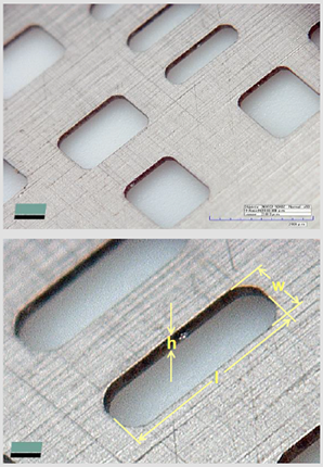
IPC-7351B recommends an Oblong
(or “Full Radius”) pad shape:
The component manufacturer’s recommend Rectangle pad shape:
PCB Libraries, Inc. recommends
a Rounded Rectangular pad shape: Paste mask stencil apertures
are laser cut with rounded corners. It makes sense that the pad shape and
stencil opening be the same. I heard of a marketing slogan
that mentioned “Rounded Rectangular pad shape is better for Lead-Free Solder”.
This is not true. All pad shapes are good with Lead-Free Solder. A better
statement would say “Rounded Rectangular pad shape is best. Period”. Rounded Rectangle pad shapes
were first introduced by the P-CAD software program 15 years ago. Then every
other CAD vendor came out with their version of the Rounded Rectangular pad
shape. The industry could not make Rounded Rectangular pad shape a standard or
even a recommendation until all CAD tools supported it. You can see that there is no
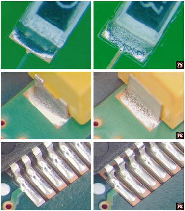
solder in the rectangular pad shape corners. The question is “Why use Rectangular
pad shape if there is no solder in the pad corners?”. The post reflow oven results
for Lead Solder on the left and Lead-Free Solder on the right. In the Library Expert software
program, the user has 100% control of the pad shape for every component family.
You also control the percentage of the pad width to auto-generate the corner
radius. You can also control the Maximum radius. However, there are some
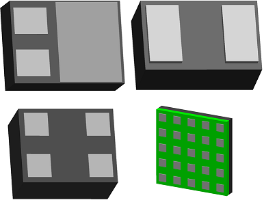
component families that are “Bottom Only” terminal leads with square or
rectangular shape. The pad size is a simple periphery around the terminal lead.
These component families include DFN, LGA and PQFN with rectangle leads and the
resulting pad shape should also be rectangular. Note: many DFN packages are
less than 2.00 mm long and the pad size is 0.50 X 0.65 mm. Very small pad and
the pad shape needs to be the same as the terminal lead shape for the best
solder result as the pad and terminal lead size are 1:1 (same size). The D-Shape pad is becoming popular, but not all CAD tools
natively support this pad shape. As a result, the D-Shape pad is created from a
copper poly shape. This makes the library part file size much larger, depending
on how many pins are in the package. This translates to the PCB Layout file
being larger too. |
|
 |
|

|
|
|
|
|
Tom H
Admin Group
Joined: 05 Jan 2012 Location: San Diego, CA Status: Offline Points: 6088 |
Post Options
Thanks(1)
Quote Reply
Posted: 18 Dec 2023 at 6:19pm |
|
Component packages are getting smaller and rectangular flat terminal leads are becoming popular. Flat square terminal leads like the Land Grid Array only require a 0.05 periphery to calculate the footprint. A 0.20 corner radius pad shape might expose the terminal lead. The terminal leads should always be on top of a pad and never be exposed outside a pad.
There is no industry recommendations for the corner radius limit and no component manufacturers (except Texas Instruments) provide any guidance for the corner radius. A recommended pattern is provided in every new Texas Instruments datasheet and every recommended pattern has rounded rectangle pad shape with a corner radius of 0.05 mm. 0.05 mm is the same radius as the paste mask stencil aperture opening cut by laser. I wish there was more guidance from assembly shops or the IPC J-STD-001 Standard, IPC-7093A, IPC-7351B or IPC-7352 regarding rounded rectangle pad shape corner radius limit, but it seems that the only industry documentation on this subject comes from Texas Instruments. Normally, a corner radius setting in a CAD tool is global to all footprint patterns. When the setting is 25% of the pad width, larger pads will have a huge corner radius and might expose the terminal lead. Whatever corner radius percentage and radius limit you choose to use is a personal setting for your PCB library. In the V24 Footprint Expert, the corner radius limit is set to 0.10 mm but users can change the value to whatever they want. |
|
|
|
|
Frank_81
New User 
Joined: 05 Jan 2024 Status: Offline Points: 2 |
Post Options
Thanks(0)
Quote Reply
Posted: 05 Jan 2024 at 2:12pm |
|
There is no industry recommendations for the corner radius limit and no component manufacturers (except Texas Instruments) provide any guidance for the corner radius.
Hi Tom - Can you share the TI document name please? Is it available online? |
|
|
|
|
Tom H
Admin Group
Joined: 05 Jan 2012 Location: San Diego, CA Status: Offline Points: 6088 |
Post Options
Thanks(1)
Quote Reply
Posted: 05 Jan 2024 at 3:02pm |
|
Texas Instruments does not have a specific document for pad shape and corner rounding.
Every TI datasheet has a "Mfr. Recommended Pattern" and the pad shapes are all rounded rectangle with a 0.05 mm radius. 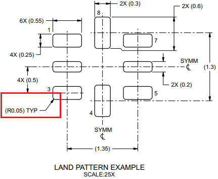 I'm seeing more and more manufacturer's recommending rounded corners. Here's a recommended pattern from Bourns. 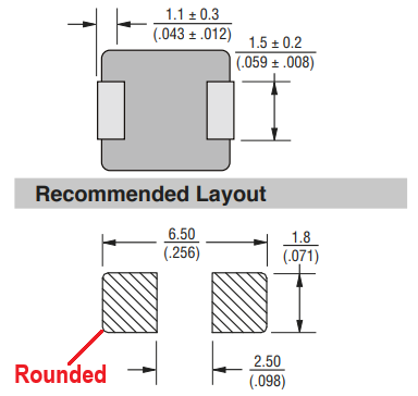 |
|
|
|
|
Frank_81
New User
Joined: 05 Jan 2024 Status: Offline Points: 2 |
Post Options
Thanks(0)
Quote Reply
Posted: 05 Jan 2024 at 3:35pm |
|
Thanks Tom for the detailed response. Appreciate you taking time to respond with details.
|
|
|
|
|
dramos
Advanced User 
Joined: 18 Feb 2021 Status: Offline Points: 101 |
Post Options
Thanks(0)
Quote Reply
Posted: 05 Mar 2024 at 7:52am |
|
Dear Tom,
I have a question around this topic. PCBLibraries started with a Corner Radius size of 25% with a limit of 0.25mm and the new release has a limit of 0.10mm. I see it as an evolution. Besides, It is in the same way that the recommendation of some Manufacturers. My question is, what you have seen to make this evolution? What you have detected on the new components/footprints to modify this value? Which is the main reason for this change? As ever, thanks a lot for your comments. Regards, dramos
|
|
|
|
|
Tom H
Admin Group
Joined: 05 Jan 2012 Location: San Diego, CA Status: Offline Points: 6088 |
Post Options
Thanks(0)
Quote Reply
Posted: 05 Mar 2024 at 9:55am |
|
The corner radius was set to 25% of the pad width with a limit of 0.25 maximum radius. We also noticed that the new mathematical model for IPC-7352 that turned off the fabrication and assembly tolerance calculated some pads to be slightly smaller (depending on the terminal tolerance). Also, there is an explosion of microminiature packages where the 0.25 corner rounding exposed package terminal leads. The metal component terminals were too close to the pad corners. You go through trial and error and test things out, but the end goal is to be safe and ensure that all terminal leads have full contact with the pad and consistent quality where all rounded corners are the same size. You get the best overall functionality with symmetrical cosmetically. PCB design is an art and the goal is to create beautiful yet functional PCB Layouts, It's also good for paste mask stencils where the aperture matches the pad shape. However, the setting is User Definable to allow you to change the default setting to whatever you want. |
|
|
|
|
dramos
Advanced User
Joined: 18 Feb 2021 Status: Offline Points: 101 |
Post Options
Thanks(0)
Quote Reply
Posted: 06 Mar 2024 at 2:11am |
|
Dear Tom,
Many thanks for your comments. Yes, the PCB designers are little painters, sculptors (jejeje) As the new IPC-7352 was downgraded to a guideline and we do not read anything strange about it in internet, we do not have bought it, but, is there a new mathematical model? I thought that was the same that we used in IPC-7351B, but with the recommendation of using for fabrication and placement tolerances 0.00 mm. (this is another topic that we will discuss another day) and we should change the negative values of our solder Joints to 0.00mm as well. Am I in a error? Best regards, david |
|
|
|
|
Tom H
Admin Group
Joined: 05 Jan 2012 Location: San Diego, CA Status: Offline Points: 6088 |
Post Options
Thanks(0)
Quote Reply
Posted: 06 Mar 2024 at 9:59am |
|
Those 2 things were major updates in IPC-7352.
The Fabrication tolerance was originally created in the 1980's to compensate for the etching process. But we all know this was unnecessary because all fabrication shops swell the outer layer features to compensate for their etching process tolerance. Appling a fabrication tolerance on a pad stack calculation and having the fabrication shop swell the outer layers is called a "Double Tolerance". It took IPC 40 years to figure that out. The Assembly tolerance was also created in the 1980's when pick and place machines required a tolerance of 1 mil (0.025). But the pick and place machine accuracy in 2024 is 0.01 mm and it might as well be 0.00 due to the 0201 chip package. Machines used in PCB Assembly and used to manufacture components are much more accurate today than 40 years ago. |
|
|
|
|
pcb0123
New User
Joined: 03 Jan 2013 Status: Offline Points: 1 |
Post Options
Thanks(0)
Quote Reply
Posted: 31 Jul 2024 at 9:12am |
|
Hi Tom,
We are curious, what are the factors that have led PCB Libraries to make the IPC-7352 approach an option, rather than the default? Is library consistency the main driver, where you don't want to impose the change on users (where it might slip past their attention) and you want the user to be fully aware they are opting in to the newer IPC-7352 approach? Other reason(s)? Thanks, Susan
|
|
|
|
|
Post Reply
|
Page 12> |
| Tweet |
| Forum Jump | Forum Permissions You cannot post new topics in this forum You cannot reply to topics in this forum You cannot delete your posts in this forum You cannot edit your posts in this forum You cannot create polls in this forum You cannot vote in polls in this forum |


 Topic Options