

|
|
3D Plus Component |
Post Reply 
|
| Author | |
AGONZ67 
Committee 

Joined: 30 Mar 2012 Status: Offline Points: 122 |
 Post Options Post Options
 Thanks(1) Thanks(1)
 Quote Reply Quote Reply
 Topic: 3D Plus Component Topic: 3D Plus ComponentPosted: 30 Oct 2015 at 5:32pm |
|
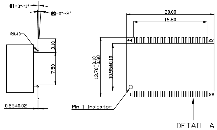
Is there a correct package type in Library Expert to create an accurate landpattern for this component? SOL was the closest I could find but this is limited to 8 pins. uploads/71/package_w4.pdf
|
|
 |
|

|
|
|
|
|
Tom H
Admin Group 

Joined: 05 Jan 2012 Location: San Diego, CA Status: Offline Points: 6096 |
Post Options
Thanks(1)
Quote Reply
Posted: 30 Oct 2015 at 9:20pm |
|
This is a unique lead form that is not registered in any standard. It would require a mfr. recommended pattern. Or I would personally calculate the pad length and spacing using the math that is noted in "What's New in IPC-7351C" - download The "Pad Length" math calculation for a Nominal Density Level is (get the pad width and pad spacing from the IPC-7351C paper):
 |
|
|
|
|
Post Reply
|
|
| Tweet |
| Forum Jump | Forum Permissions You cannot post new topics in this forum You cannot reply to topics in this forum You cannot delete your posts in this forum You cannot edit your posts in this forum You cannot create polls in this forum You cannot vote in polls in this forum |


 Topic Options