

|
|
Manufacturer Recommended Patterns |
Post Reply 
|
| Author | |
Nick B 
Admin Group 

Joined: 02 Jan 2012 Status: Online Points: 2066 |
 Post Options Post Options
 Thanks(0) Thanks(0)
 Quote Reply Quote Reply
 Topic: Manufacturer Recommended Patterns Topic: Manufacturer Recommended PatternsPosted: 15 Aug 2026 at 11:00am |
|
All non-standard packages must use the recommended manufacturer pattern. The misconception that simply using the manufacturer recommended pattern will keep you safe is enough to get you in serious trouble, and over time, create mayhem in your CAD library. You need much more than the recommended pattern for a reliable PCB design! Most component manufacturers provide recommended solder patterns in their datasheets, but there are two major issues you need to consider:
Here is a representation of a Manufacturer Recommended Pattern with rounded rectangle pad shape. All component manufacturers (except Texas Instruments) recommended rectangle pad shape. However, paste mask stencil apertures are laser cut with rounded corners. 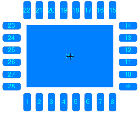 This is obviously missing the six critical drafting outlines. Traditionally, these have been manually created with a plethora of inconsistent rules that get adjusted over time:
It takes more time to manually add all the necessary Drafting Outlines than it does to create the Manufacturer Recommended Pattern, and these are just as important as the pattern itself! All drafting outline widths and spacings are defined in your personal master Options file. This guarantees consistent quality throughout your entire CAD library. You can also turn off any drafting outline that you do not want in your CAD library, but easily “bring it back” if you decide later that you need it! This is your end goal, read on for details how to reach it: 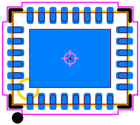 The Component Outline is crucial for accurate assembly placement and helps ensure your components fit properly on the board. It helps with verification during visual inspections, and facilitates repair, rework, and future updates to the design. 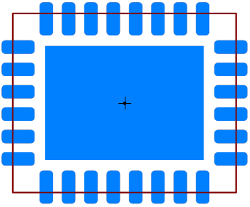 The Terminal Outlines are likewise critically important. They represent where on the metal terminal leads the physical package makes contact to the PCB. These are essential for reliable soldering and proper electrical connectivity. Each terminal lead outline must be entirely located on a pad. If the pad is not 100% on a metalized terminal outline, then the manufacturer’s recommended pattern is not good, and you will get a bad solder connection. 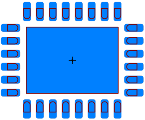 The Silkscreen Outline enables proper component orientation and should be created so that it’s visible after assembly. Silkscreen outlines should not be placed under the package body – they are useless there and could potentially lift low profile or micro-miniature components off the PCB surface resulting in poor solder joints. The silkscreen data includes a post assembly inspection dot located by Pin 1, which helps with final assembly inspection. 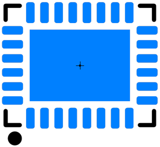 The Assembly Outline is a closed polygon. A chamfered corner is located by Pin 1 if the component is polarized or cannot be inverted during assembly. The assembly outline is important because it provides clear reference points for automated pick-and-place machines. A well-defined Assembly Outline also facilitates design verification and quality control. 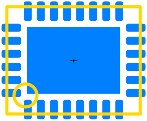 The Courtyard Outline is extremely important in defining the required minimum clearance area required for a component, ensuring there is no interference with neighboring components during assembly or operation. The ideal shape is contoured around the package body and pads, which is the default setting in the Footprint Expert. The courtyard excess value for Package Body and Pads can be set separately. 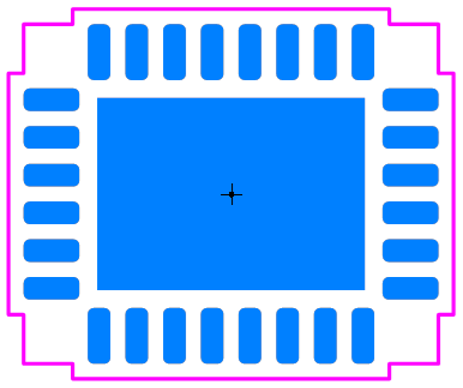 The Origin Outlines are placed on an independent layer. The size & outline width are user definable. Accuracy is essential for accurate alignment because it serves as a reference for positioning the component on the PCB. A precise origin simplifies machine programming and enhances design portability across tools. 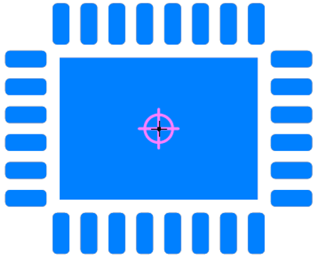 Datasheet dimensional tolerances are usually a conservative envelope rather than the real production distribution. If/when measurement data shows the parts are tightly controlled – Six Sigma quality levels – designing footprint geometry using nominal dimensions instead of worst-case maximum material condition can give us a reliable solder joint and provide space for routing. Having real measurement distribution data could support a change toward using nominal measurements. For standard components, we can round the corners of any rectangular pads with a ~0.05 mm corner radius. This eases routing with little to no reliability trade-off, and on tight-pitch QFNs it buys extra corner clearance, which reduces the chance of solder mask slivers. If the manufacturer's QFN pads are a D-shape/finger shape with a full round on the heel side nearest the EPAD, match that shape for the same reason – there is very little downside, and it helps corner clearance. Footprint Expert can output the terminal outlines and show where the physical part lands on the pads. Adding a 3D model to visually confirm footprint-to-component compatibility is also very helpful – Footprint Expert generates both the footprint and the 3D model for standard packages on the same origin and orientation. For non-standard parts, finding the most detailed manufacturer model available and stacking it against the pattern in CAD is another check I'd recommend. A few package types genuinely benefit from following the manufacturer's recommendation. Example: Texas Instruments (TI) provides highly detailed recommended patterns for every Case Code they develop. Their pad stack patterns are almost predicable because they use the same terminal lead width and length for each pin pitch for each component family. TI provides solder mask data that always has a solder mask web between the pads. It’s as if they created their terminal lead widths intentionally to avoid gang masking rows of pins. The paste mask apertures for thermal pads always have a 0.20 mm aperture gap, a 0.05 mm corner radius on every aperture and they provide 80% paste mask coverage. They recommend a 0.05 mm corner radius on every pad stack while most component manufacturers recommend a rectangular pad shape and no solder or paste mask recommendations. TI is one of the most organized component manufacturers with consistent quality. Their Case Code packages are used by multiple part numbers, and many TI Case Codes are assigned to thousands of part numbers. Thermal-Pad Paste Mask: Manufacturers typically recommend a paste pattern other than 1:1 with the metallized area, because excessive paste floats and rotates the part during reflow, risking pin-to-pin shorting and open perimeter joints. IPC-7093 covers the windowpane/array aperture with coverage commonly in the ~50–80% range. Footprint Expert hits the coverage target through the options file, which saves hand-drawing each paste block. Tight-tolerance Guide Pins or Press-Fit Pins: Go with the manufacturer's recommendation. Guide pins and press-fit finished-hole size and tolerance are manufacturer-specific (compliant-pin design) and should come straight from their drawing. High-Power Pads: The recommended pad may be larger than the calculated one to add heat dissipation and reduce thermal-cycling fatigue. Here we can solder mask-define the pad: the copper layer uses the manufacturer's larger recommended size for heat spreading and mechanical robustness, and the solder mask opening uses the Footprint Expert-calculated land, since the mask edge is what defines the solderable area. High-Voltage Applications: The recommended pads may be spaced further apart than the Footprint Expert lands. Use IPC-2221B to confirm the pattern is acceptable for the given voltage. RF Components: Follow the manufacturer's recommendation as closely as possible. These almost always ship with an evaluation board demonstrating tested performance across the listed parameter range, which is a reliable starting point. RF engineers typically begin from that recommendation and modify based on bench data or EM simulation for their specific needs. Die Components: Also, a case to follow the manufacturer closely – though these often have no recommendation. Working with die means an advanced process/fab house by definition, so we can build the pad stack 1:1 with the die-bump metallization with no solder mask expansion, use the CAD tool's layer capabilities to assign double-sided features that must count electrically in the schematic, and define plated or non-plated contours for cavity-mounted applications. |
|
 |
|

|
|
|
|
|
Post Reply
|
|
| Tweet |
| Forum Jump | Forum Permissions You cannot post new topics in this forum You cannot reply to topics in this forum You cannot delete your posts in this forum You cannot edit your posts in this forum You cannot create polls in this forum You cannot vote in polls in this forum |


 Topic Options