The pad stack consists of combinations of letters and numbers that represent shape, or dimensions of lands on different layers of printed boards or documentation. The name of the pad stack needs to represent all the various combinations. These are used in combination with the land pattern conventions defined herein according to the rules established in the IPC-2220 Design standards.
All dimensions in this Naming Convention section are in "mm", unless otherwise noted.
The first part of the pad stack convention consists of a land shape. There are ten basic land shape identifiers. Note: All alphabetical characters are "lower case". This helps discriminate numeric values.
Basic Land Shape Letters
- r = Rectangle
- rr = Rounded Rectangle
- cr = Chamfered Rectangle
- b = Oblong
- d = D Shape (Square on one end and Circular on the other end)
- c = Circular
- s = Square
- rs = Rounded Square
- cs = Chamfered Square
- u = User Defined Contour (Irregular Shape)
Pad Stack Defaults
- Solder Mask is 1:1 scale of the land size
- Paste Mask is 1:1 scale of the land size
- The Assembly Layer land is 1:1 scale of the land size
- Inner Layer Land is the same shape as the outer layer land
- The Primary and Secondary lands are the same size
- The inner layer land shapes are Circular
- Vias are Circular
- Thermal ID, OD and Spoke Width sizes follow the IPC Level A, B or C
- Plane Clearance Anti-pad size follows the IPC Level A, B or C
- Thermals have 4 spokes
- Mounting Holes are Circular
Note: Every board fabricator’s ability to register solder mask is different. The 1:1 scale solder mask covers the variation, and so long as manufacturers are building to specs such as IPC-6012 that say you can’t have mis-registration of the solder mask.
Illegal characters that cannot be used (Microsoft requirement) include " " , ; : / \ [ ] ( ) . { } * & % # $ ! @ ^ =
Examples utilizing the pad stack naming convention (all values are in metric units)
Note: Every number goes two places to the right and as many as needed to the left of the decimal
Examples: 1150 = 11.50 or 11500 μm, 150 = 1.50 or 1500 μm, 15 = 0.15 or 150 μm
- c150h90 where "c" denotes a Circular land with a 1.50 diameter and H denotes a hole size of 0.90
- c130_95 Donut pad where "c" denotes a Circular land with a 1.30 OD diameter and 95 denotes the ID diameter
- c130_95hn70k147 Donut pad - "c" denotes a Circular land with a 1.30 OD diameter and 95 denotes the ID diameter and hn70 denotes hole, non-plated 0.70 diameter and k147 denotes a keep-out 1.47 diameter
- v50h25 where a "v" denotes a via with a 0.50 land (default Circular land) and h denotes a 0.25 hole
- s150h90 where "s" denotes a 1.50 Square land and h denotes a hole size of 0.90
- s350 where "s" denotes a square SMT land size of 3.50
- r200_100 where "r" denotes a Rectangular SMT land 2.00 land length X 1.00 land width
- b300_150 where "b" denotes a SMT Oblong land size of 3.00 X 1.50
- b400_200h100 where "b" denotes an Oblong land size of 4.00 length X 2.00 width and 1.00 hole
- d300_150 where "d" denotes land with one circular end and one square end (looks like a D) 3.00 X 1.50
- v30h15l1-3 where "v" denotes a 0.30 blind via with 0.15 Hole; 1 is the starting layer, 3 is the end layer
- r200_100r5 = Rounded Rectangular 2.00 X 1.00 X 0.05 radius corners
- r200_100c10 = Chamfered Rectangular 2.00 X 1.00 X 0.10 chamfered corners
- v30h15l3-6 where "v" denotes a 0.30 buried via with 0.15 Hole; 3 is the starting layer, 6 is the end layer
Note: It is assumed that the through-hole pad stack has the same value as the mounted layer size and shape for -
- Inner Layer
- Opposite Side
- Solder Mask
- Solder Paste
- Assembly Layers
It is also assumed that the "Plane Clearance" and "Thermal Relief" data follows the through-hole convention guidelines defined in the IPC-2221 and IPC-2222 standards.
Modifiers that are used when pad stack features are different than the defaults
These are the "Variants" or "Modifiers" that go after the basic pad stack naming convention.
These are used when the User needs to change the pad stack default values either by a different dimension or a different shape. In instances where shapes are different this becomes a two letter code with the modifier first followed by the land shape letter.
- n = Non-plated Hole
- z = Inner Layer land dimension if different than the land on primary layer
- x = Special modifier used alone or following other modifiers for lands on opposite side to primary layer land dimension
- t = Thermal Relief; if different than IPC standard pad stack – tid_od_sw for 4 spoke default
- m = Solder Mask if different than default 1:1 scale of land
- p = Solder Paste if different than default 1:1 scale of land
- a = Assembly surface land if different than default 1:1 scale of land
- y = Plane Clearance (Anti-pad) if the value is different than the Thermal OD
- o = Offset Pad & Solder Mask with the same + / - value
- om = Offset Solder Mask Only + / - value
- op = Offset Paste Mask only + / - value
- k = Keep-out
- r = Radius for Rounded Rectangular Land Shape
- c = Chamfer for Chamfered Rectangular Land Shape
Shape change is the last letter in the string prior to the dimension.
Other usage of the pad stack naming convention
USE of letter v: Vias can be named using the pad stack naming convention. Because most vias use lands that are circular in shape, the letter "v" will be used in place of the letter "c" in the pad stack naming convention. If this is not true the modifiers can be added after the letter "v" to signify shape or dimensional changes to this default.
USE of letter w: In addition to Vias the pad stack naming convention can also be used for defining mounting holes. The letter "w" shall be used to define the mounting hole characteristics and any associated lands used for the surface lands (either plated or un-plated)
Examples of double character modifiers:
- ts = Thermal Square; if different than the top side land shape and dimensions
- sw = Thermal spoke width
- zs = Inner Layer Land Shape is Square (Note: The default is circular)
- m0 = No Solder Mask
- mxc = Solder Mask Opposite Side Circular
- mx0 = Solder Mask Opposite Side No Solder Mask
- p0 = No Paste Mask
- xc = Opposite Side Circular
- vs = Via with Square land
- hn = Non-plated Hole
Modifier Example for Through-hole:
- s150h90zs150 = where "s" is Square 1.50 land with 0.90 Hole with 1.50 inner (Z) Layer Square land
- c150h90zc150 = where "c" is Circular 1.50 land with 0.90 Hole with 1.50 inner (Z) Layer Circular land
Modifier Examples for Vias:
- vs50h25 where "vs" denotes a 0.50 Square Via with a 0.25 Hole
- v50h25xs70 where "v" is 0.50 Circular Via with 0.25 Hole and 0.70 Square land on opposite side
Chamfered & Rounded corner modifiers are used to indicate which corner(s) are modified. Order of precedence has been given to the first 4 modifiers.
Modifiers:
- bl – bottom left
- br – bottom right
- ul – upper left
- ur – upper right
- ulr – upper left & right
- blr – bottom left & right
- ubl – upper and bottom left
- ubr – upper and bottom right
Rounded and Chamfered lands in "one corner" Modifier Examples:
- r100_200rbl50 = rectangular land 1.00 x 2.00 with 0.50 radius for rounded corner in bottom left corner
- r100_200rbr50 = rectangular land 1.00 x 2.00 with 0.50 radius for rounded corner in bottom right corner
- r100_200rul50 = rectangular land 1.00 x 2.00 with 0.50 radius for rounded corner in upper left corner
- r100_200rur50 = rectangular land 1.00 x 2.00 with 0.50 radius for rounded corner in upper right corner
- r100_200cbl50 = rectangular land 1.00 x 2.00 with 0.50 chamfer for chamfer corner in bottom left corner
- r100_200cbr50 = rectangular land 1.00 x 2.00 with 0.50 chamfer for chamfer corner in bottom right corner
- r100_200cul50 = rectangular land 1.00 x 2.00 with 0.50 chamfer for chamfer corner in upper left corner
- r100_200cur50 = rectangular land 1.00 x 2.00 with 0.50 chamfer for chamfer corner in upper right corner
Examples of a square land with 3 rounded and 1 chamfered corner (for Thermal Pad)
- s300p190r25cul50 = square 3.00 land, square paste 1.90, corner radius 0.25, upper-left chamfer 0.50
- s300p190r25cbl50 = square 3.00 land, square paste 1.90, corner radius 0.25, bottom-left chamfer 0.50
Chamfered and Rounded Rectangular with all four corners chamfered does not need a corner modifier. Modifier Examples with Rounded Rectangle Land Shape:
- r200_100r50 = rectangular land 2.00 x 1.00 with 0.50 radius for rounded corners in all 4 corners
- r200_100c50 = rectangular land 2.00 x 1.00 with 0.50 chamfer for chamfered corners in all 4 corners
Examples of a pad stack with Circular land with hole using various modifiers
- c150h90 = Default pad stack with a 1.50 circular land with a 0.90 hole (no modifiers used)
- c150hn90 = Default pad stack with a 1.50 circular land with a 0.90 non-plated hole (no modifiers used)
- c150h90z140 = Inner layer land is smaller than external lands 1.40 or 0.10 smaller
- c150h90z140x170 = Opposite side land is larger than top side land 1.70 or 0.20 larger
- c150h90z140x170m165mx185 = Solder mask opening for top and bottom lands 0.15 larger for each
- c150h90z140x170m165mX185a200 = Assembly drawing land in 0.50 larger than 1.50 primary land
- c150h90z140x170m165mx185a200y300 = Plane clearance anti-pad diameter is 3.00
- c150h90z140x170m165mx85 = Solder mask encroachment on opposite land by 0.65 smaller
- c150h90m165 = adding a solder mask opening of 1.65 diameter or 0.15 larger than land
- c150h90t150_180_40 = Thermal ID 1.50, OD 1.80, Spoke Width 0.40, Anti-pad 1.80
- c150h90t150_180_40y200 = Anti-pad 2.00 (because the size is different than the Thermal OD)
- c150h90t150_180_80_2 = Spoke Width 0.80 with 2 Spokes
- c150h90m165t150_180_40 = Solder Mask 1.65
Examples of a pad stack with Oblong land with Slotted Hole
- Sample - b = Oblong Land Shape then "X" dimension (length) then Underscore _ "Y" dimension (width)
- b400_200h300_100 = Oblong land 4 length X 2 width with slotted hole size 3 X 1
- b400_200hn300_100 = Oblong land 4 X 2 with non-plated slotted hole size 3 X 1
Examples of a SMT pad stack land using various modifiers
- b300_150 = Default pad stack with a 3.00 length and 1.50 width land (no modifiers used)
- b300_150m330_180 = Solder Mask is 0.30 larger than the land on all sides
- b300_150m330_180p240_140 = Solder Paste is smaller by 0.10 width and 0.60 length
- b300_150b-50 = Oblong Land 3.00 X 1.50 w/Offset Origin negative 0.50
- r400_200pb430_230 = Rectangle SMT land 4.00 X 2.00 with an Oblong Paste Mask size of 4.30 X 2.30
Example of Thermal Pads for QFN, SON, QFP and SOP
Square Configurations
s480p4s152 = 4.80 Square Land with 4 Paste Mask Squares 1.52 each
s480p4s152cul50 = 4.80 Square Land with 4 Paste Mask Squares 1.52 each with 0.50 Chamfer in Upper Left corner
s480p4s152cul50r25 = 4.80 Square Land with 4 Paste Mask Squares 1.52 each with 0.50 Chamfer in Upper Left corner with 0.25 corner Radius
Example of a Mounting Hole
- w700h400z520m720 = This is a Plated Through Mounting hole for a #6-32 screw using a 4.00 diameter hole and having a circular 7.00 land on the primary and secondary side of the board, with a solder mask clearance that is 0.20 larger than the 7.20 land. The internal lands are smaller that the external and are also circular 5.20 in diameter.
- w700hn400z520m720 = Non-plated version
Example of a Local Fiducial for Fine Pitch SMT Components
- c100m200k200 = Circular Land 1.00 with Solder Mask 2.00 with Keep-out 2.00
- s100m200k200 = Square Land 1.00 with Solder Mask 2.00 with Keep-out 2.00
Example of Proportional Plated Through-hole Pad Stack
- c150h100 = 1.50 circular pad with 1.00 hole with 1.50 solder mask with 1.50 plane clearance with 1.50 assembly outline with Thermal Relief w/4 spokes 0.40 width with ID 1.50 and OD 1.80
Example of Proportional Non-plated Through-hole Pad Stack
- c100hn150 = 1.00 circular pad with 1.50 hole "non-plated" with 1.50 solder mask with 2.35 plane clearance with 2.10 keep-out




 Post Options
 Thanks(0)
 Quote
Quote  Topic: IPC-7352 Pad Stack Naming Convention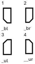








 Topic Options