

|
|
Through-hole Terminals |
Post Reply 
|
| Author | |
Nick B 
Admin Group 

Joined: 02 Jan 2012 Status: Offline Points: 2066 |
 Post Options Post Options
 Thanks(0) Thanks(0)
 Quote Reply Quote Reply
 Topic: Through-hole Terminals Topic: Through-hole TerminalsPosted: 15 Aug 2026 at 11:00am |
|
A through hole pad stack is a set of Printed Circuit Board features that define a plated or non-plated, drilled hole that: 1. accommodates a component terminal lead; 2. Provides or prevents a connective path between layered circuitry; or both. Elements of a Through-hole Pad Stack 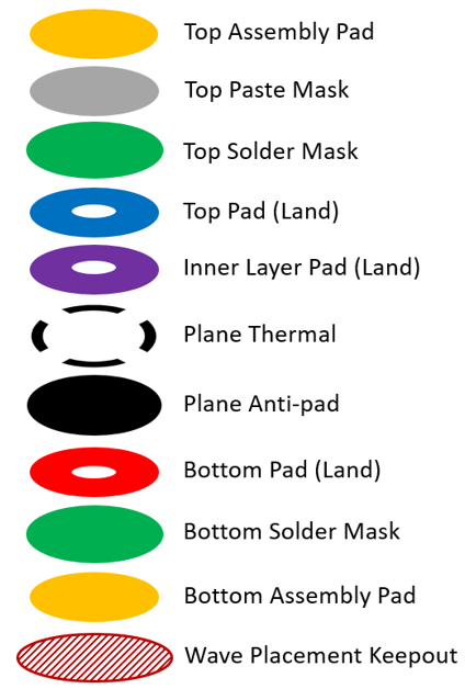 Pad on Assembly Layer This is a unique, user selectable pad stack option in that it is defined as a Component option. 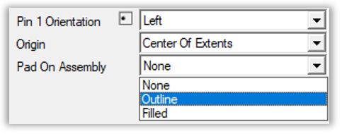 When Outline is selected, graphics, created from the Top and Bottom pads, are added as drawing line elements on the respective footprint Assembly Layers. When Filled is selected, regular filled pads are added to the terminal pad stack on the Top and Bottom Assembly layers. Footprint Expert Options for Through-hole Pad Stacks 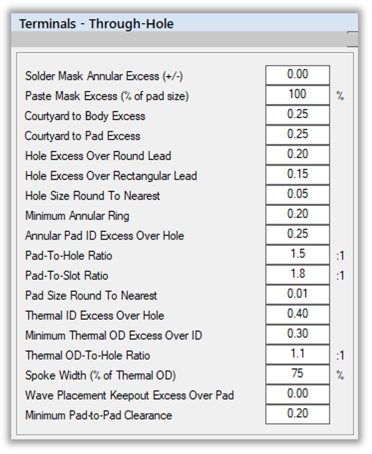 Solder and Paste Mask Excess The Solder Mask Excess option sets the size of the solder mask pad relative to the top or bottom pads, respectively. The value is expressed as either over (pad plus excess) or under (pad minus excess). Paste Mask, when applied to through-hole pad stacks and referred to as "Pin-in-Paste", is an advanced soldering technique that integrates through-hole and surface mount components in a single reflow pass. This method involves depositing solder paste inside through-hole vias and pads before component placement, allowing for soldering through-hole pins and the PCB in one step. Paste mask size is typically smaller than their associated and expressed as percentage of its associated pad size. 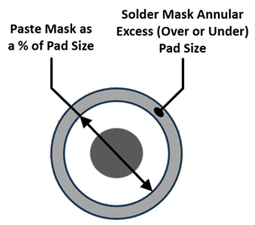 Courtyard Clearance to Pad and Body While these values appear as pad stack options, they don’t appear anywhere as physical features in the pad stack itself. Their effect is only noticeable in the courtyard outline spacing surrounding the footprint. A value of zero applied to either option results in a courtyard with no clearance to that option. 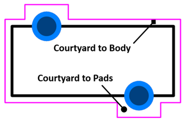 Hole Excess over Lead There are two possible value choices for this option. Hole Excess to Round or Excess to Square/Rectangular leads. The excess value sets a round hole diameter equal to the round lead diameter or the square/rectangular lead diagonal, plus the specified hole over lead clearance. Example: square lead = 0.50; lead diagonal = 0.707; hole over lead = 0.15; hole diameter = 0.707 + 0.15 = 0.857. 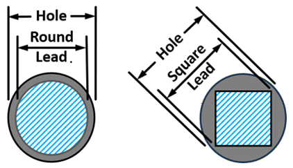 Hole Size Round To Nearest This option is applied the result of the hole calculation to force a finished hole value to be rounded up so as to be evenly divisible by this value. Setting this value to zero will allow a hole size to round off to the Design Options units decimal place setting. Example: round 0.857 up to the nearest 0.05 = 0.90. Annular Ring The Annular Ring is a pad with an inner diameter that maintains a clearance to a plated or non-plated hole. It is defined by two values: a pad outer diameter (or length and width) and a uniform excess spacing of the inner pad dimensions to the hole perimeter. 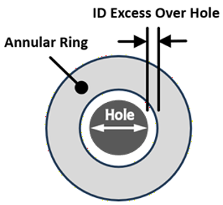 Pad-To-Hole and Slot Ratios Optional ratios can be applied to pad stack calculations that provide an additional robustness that grows in proportion to the hole or slot size. In practice, the pad size is initially derived as ratio to the hole size then other settings (such as Minimum Annular Ring, etc.) can be applied as required. The effect of ratios on pad size is illustrated below. Hole and slot sizes shown are equal and all other through-hole option settings are the same. 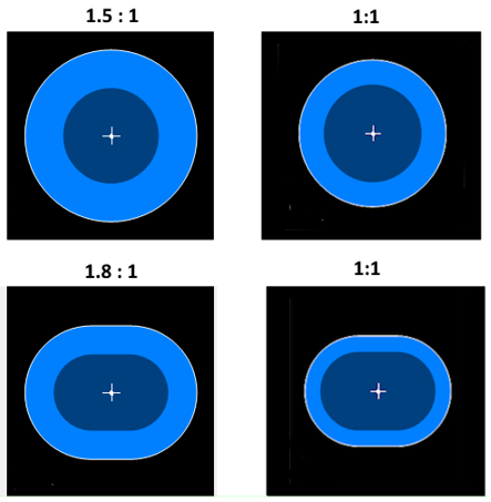 Example (round hole and pad): Hole = 0.70; Pad = Hole x Ratio = 0.70 x 1.5 = 1.05. Pad Size Round-To-Nearest This option is applied to the result of the pad calculation to force a finished pad value to be rounded off so as to be evenly divisible by this value. Setting this value to zero will allow a pad size to round off to the Design Options units decimal place setting. Example: round 1.05 up to the nearest 0.1 = 1.10. Thermal Relief A Thermal relief, also called a thermal pad, is a pattern of copper strips, or ‘spokes’ connecting a PCB pad, across a void, to a large copper area, such as a ground or power plane. Unlike a solid connection, a thermal relief limits heat transfer, preventing the copper plane from acting as a heat sink that could result in a ‘cold’ solder joint. Thermal Relief Options 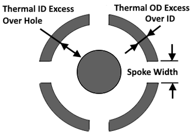 Thermal ID Excess Over Hole Defines the conductive clad space between the hole and the thermal void inner diameter. Thermal OD Excess Over Thermal ID Determines the size of the non-conductive void between the inner clad and outer plane. Thermal OD and Thermal OD-to-Hole Ratio Thermal Outer Diameter is the extent of the Thermal Pad Stack Layer and calculated as: Thermal ID Over Hole + Thermal OD Over ID + (Hole x Ratio). Example: Thermal OD = 0.40 + 0.30 + (0.70 x 1.1) = 1.47. Anti-pad An Anti-pad is a design feature that creates a plane clearance area around a plated or non-plated through-hole. The anti-pad void serves to avoid unintended connections between vias, traces and layers; improve solderability and reduce thermal stress during the assembly process. In Footprint Expert, the Anti-pad is calculated to equal Thermal OD. Thermal Spoke Width Width is calculated as: Spoke Width = Spoke Width % x (Thermal OD / 4), Example: Spoke Width = 0.75 x (1.47 / 4) = 0.28 Wave Placement Keep-out Excess Over Pad A wave placement keep-out is a non-routable region on the bottom of a PC board that prevents solder from flowing into certain areas, such as component pads, mounting holes, fiducials or high-voltage zones during a wave soldering process. The size of a Wave Placement Keep-out is completely up to the footprint designer based on a component’s application. The size is simply defined as an excess to be added to the bottom pad. 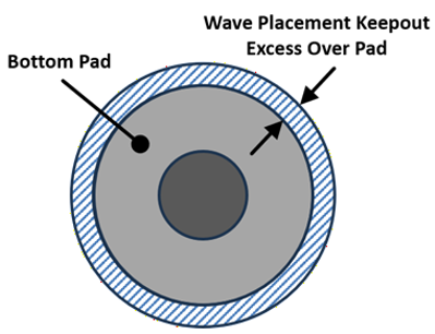 |
|
 |
|

|
|
|
|
|
Post Reply
|
|
| Tweet |
| Forum Jump | Forum Permissions You cannot post new topics in this forum You cannot reply to topics in this forum You cannot delete your posts in this forum You cannot edit your posts in this forum You cannot create polls in this forum You cannot vote in polls in this forum |


 Topic Options