|
|
IPC-7352 Mathematical Model |
Post Reply 
|
| Author | |
Tom H 
Admin Group 

Joined: 05 Jan 2012 Location: San Diego, CA Status: Offline Points: 6072 |
 Post Options Post Options
") Thanks(0) Thanks(0)
 Quote Reply Quote Reply
 Topic: IPC-7352 Mathematical Model Topic: IPC-7352 Mathematical ModelPosted: 16 Apr 2026 at 5:06pm |
|
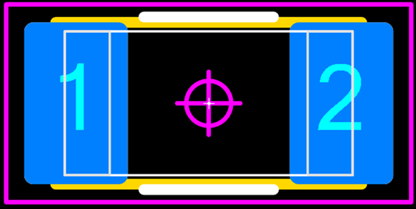
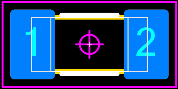
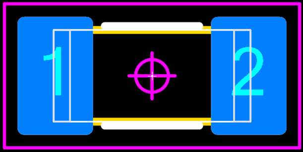
This is an example of a 1206 Chip Resistor package. Dimensions: H = 1.40, D = 3.20 ±0.20, E = 1.60 ±0.20, L = 0.50 ±0.25 The IPC-7352 mathematical model includes the D, E and L dimensions and tolerances and the solder joint goal settings for Toe = 0.35, Heel = 0.00, Side = 0.00 Resulting pad size rounded to 2 places is – L 1.15 x W 1.80 x G 1.80 The resulting pad stack pattern must have the terminal leads on the pad stack in these conditions: The Nominal Material condition of the component package & Nominal Terminal.
The Minimum Material condition of the component package & Nominal Terminal.
The Maximum Material condition of the component package & Nominal Terminal.
The Minimum Material condition of the component package & Minimum Terminal.
The Maximum Material condition of the component package & Maximum Terminal.
The resulting pad stack must have terminal leads on the pad stack regardless of every possible Material Condition possible to pass assembly inspection and meet the requirements set forth in the IPC J-STD-001 Standard and the IPC-7352 Guideline in Figure 3-3 Profile Dimensioning. i.e.: regardless of the Component Package and Terminal Lead Material Condition, the Terminal Lead must never be exposed outside the calculated pad stack. This is proof that the V24 Footprint Expert mathematical model illustrated in the IPC-7352 guideline achieves that goal. Note: most component packages are created in the Nominal Material Conditions. The package tolerances play a key role in the resulting pad stack. Nominal Package Dimensions & no Package Tolerances. 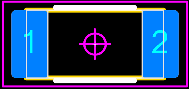 See IPC-7352 for the full mathematical model data.  PCB Footprint Expert Simplify your PCB design process with the Footprint Expert, the ultimate tool - it automatically applies this mathematical model and automates footprint and 3D model creation. Automation helps ensures accurate, consistent, reliable footprints with minimal introduction of human error. Let the Footprint Expert handle your CAD library so you can focus on creating flawless PCB designs faster and more efficiently! Get your FREE Footprint Calculator or Footprint Expert Evaluation License: Call: 847-557-2300 |
|
 |
|

|
|
|
|
|
Post Reply
|
|
| Tweet |
| Forum Jump | Forum Permissions You cannot post new topics in this forum You cannot reply to topics in this forum You cannot delete your posts in this forum You cannot edit your posts in this forum You cannot create polls in this forum You cannot vote in polls in this forum |


 Topic Options