|
|
Metric PCB Design Tips |
Post Reply 
|
| Author | |
Tom H 
Admin Group 

Joined: 05 Jan 2012 Location: San Diego, CA Status: Offline Points: 5943 |
 Post Options Post Options
") Thanks(0) Thanks(0)
 Quote Reply Quote Reply
 Topic: Metric PCB Design Tips Topic: Metric PCB Design TipsPosted: 14 Apr 2022 at 9:16am |
|
Congratulations! You'll find out really quick that the metric system is superior to imperial units. I have a personal guarantee that if you use these rules and do 5 PCB designs in metric, it will be impossible for you to switch back to imperial, because you will discover the beauty of the metric system and the ugliness of the imperial system. Here are the things you need to be concerned about:
i.
Line Width and Gap for Silkscreen 0.15
ii.
Line Width for Assembly 0.10
iii.
Line Width for Courtyard 0.05
iv.
SMD Pad Length & Width
v.
Pad placement
vi.
PTH pad and hole diameters vii. Note: the worst metric SOP/QFP/QFN/SON is a 0.65 mm pitch. This screws up a great PCB layout. Be on the lookout.
i.
Big parts snap to 1.00 mm grid
ii.
Medium parts snap to 0.50 mm grid iii. Small parts snap to 0.10 mm grid
i.
Best Signal Trace Width = 0.10 mm – this allows
differential pairs for a 1.00 mm pitch BGA
ii.
Power Trace Widths = 0.20, 0.30, 0.40, 0.50,
etc.
iii.
Routing Grid = 0.05 mm
iv.
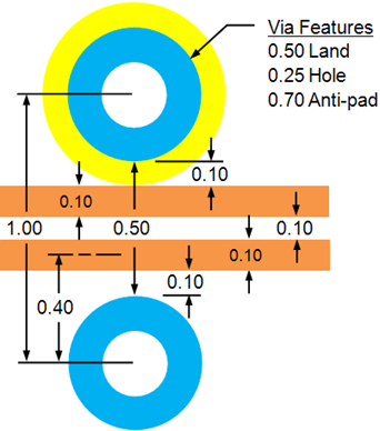
Via Pad Size = 0.50 & Via Hole Size = 0.25
v.
SMD Via Fanout should snap to a 0.10 mm grid if
possible |
|
 |
|

|
|
|
|
|
Post Reply
|
|
| Tweet |
| Forum Jump | Forum Permissions You cannot post new topics in this forum You cannot reply to topics in this forum You cannot delete your posts in this forum You cannot edit your posts in this forum You cannot create polls in this forum You cannot vote in polls in this forum |


 Topic Options