

|
|
Paste Mask Rules For Thermal Pads |
Post Reply 
|
| Author | |
manu 
Active User 
Joined: 29 Nov 2018 Status: Offline Points: 25 |
 Post Options Post Options
") Thanks(0) Thanks(0)
 Quote Reply Quote Reply
 Topic: Paste Mask Rules For Thermal Pads Topic: Paste Mask Rules For Thermal PadsPosted: 20 Mar 2019 at 4:16am |
|
Hello,
What are the exact rules for the thermal pad solder mask ? I know that it is 50% of the pad but from what size the mask is divided by 4 or more rectangles ? And what is the rule for the distance between these small rectangles? and the distance between these rectangles and the edge of the copper pad ? Thanks in advance.
|
|
 |
|

|
|
|
|
|
Tom H
Admin Group 

Joined: 05 Jan 2012 Location: San Diego, CA Status: Offline Points: 5941 |
Post Options
Thanks(0)
Quote Reply
Posted: 20 Mar 2019 at 8:36am |
|
The Thermal Tab Rules are located in the "Preferences > Rules" section of Library Expert.
You define the Thermal Tab values that are best for you to create a custom library that matches your preferences. Solder Mask Defined Thermal Pads are a new IPC-7093A standard. See this forum post - |
|
|
|
|
Tom H
Admin Group
Joined: 05 Jan 2012 Location: San Diego, CA Status: Offline Points: 5941 |
Post Options
Thanks(0)
Quote Reply
Posted: 27 Dec 2019 at 4:19pm |
|
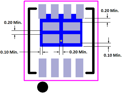
Here is an image of the Minimum paste mask aperture spacing rules for a SON package with a Thermal Pad that intersects with a row of pins.
 |
|
|
|
|
Post Reply
|
|
| Tweet |
| Forum Jump | Forum Permissions You cannot post new topics in this forum You cannot reply to topics in this forum You cannot delete your posts in this forum You cannot edit your posts in this forum You cannot create polls in this forum You cannot vote in polls in this forum |


 Topic Options