

|
|
CM Chip Inductor (4-Lead) |
Post Reply 
|
| Author | |
Tom H 
Admin Group 

Joined: 05 Jan 2012 Location: San Diego, CA Status: Offline Points: 5804 |
 Post Options Post Options
") Thanks(0) Thanks(0)
 Quote Reply Quote Reply
 Topic: CM Chip Inductor (4-Lead) Topic: CM Chip Inductor (4-Lead)Posted: 22 Oct 2014 at 10:34am |
|
Murata does not have a recommended pattern in their datasheet - http://search.murata.co.jp/Ceramy/image/img/PDF/ENG/L0114S0133DLW21S.pdf I would recommend a 0.1 mm periphery around the component lead. This part would take 3 minutes to create in the Library Expert "FP Designer". |
|
 |
|
|
|
|
Snakeeater
New User 

Joined: 25 Mar 2014 Location: Canada Status: Offline Points: 2 |
Post Options
Thanks(0)
Quote Reply
Posted: 22 Oct 2014 at 8:51am |
|
Hello,
Looking for input on constructing the following component: It is a Common Mode Chip Inductor (4-Pins, 0805) DLW21SN900HQ2L 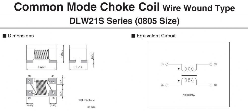 I was thinking it would fall into the Chip Array family, or possibly the DFN 4-Lead. Would someone kindly steer me in the right direction? Thank you in advance, Iain |
|
|
|
|
Post Reply
|
|
| Tweet |
| Forum Jump | Forum Permissions You cannot post new topics in this forum You cannot reply to topics in this forum You cannot delete your posts in this forum You cannot edit your posts in this forum You cannot create polls in this forum You cannot vote in polls in this forum |


")


 Topic Options