

|
|
Why is Gang Mask shape option removed? |
Post Reply 
|
Page 12> |
| Author | |
Tom H 
Admin Group 

Joined: 05 Jan 2012 Location: San Diego, CA Status: Offline Points: 5798 |
 Post Options Post Options
") Thanks(0) Thanks(0)
 Quote Reply Quote Reply
 Topic: Why is Gang Mask shape option removed? Topic: Why is Gang Mask shape option removed?Posted: 10 Jan 2025 at 11:44am |
|
We fixed the rounding issue for calculating Gang Solder Mask.
The Gang Mask code was written so the Minimum Pad to Pad had to be greater than the value entered. Adding 0.001 to the Minimum Pad to Pad worked. But now it works with the actual value (not greater than the value). We also added a new Forum post regarding this subject: The V25.03 Footprint Expert pre-release will be available next week. Thank you for reporting this issue. |
|
 |
|
|
|
|
Tom H
Admin Group
Joined: 05 Jan 2012 Location: San Diego, CA Status: Offline Points: 5798 |
Post Options
Thanks(0)
Quote Reply
Posted: 07 Jan 2025 at 4:41pm |
|
More information regarding the Nominal Calculation Mode:
|
|
|
|
|
ulissescastro
Active User 
Joined: 23 Feb 2022 Status: Offline Points: 18 |
Post Options
Thanks(0)
Quote Reply
Posted: 07 Jan 2025 at 4:34pm |
|
Thanks. All good now...
|
|
|
|
|
Tom H
Admin Group
Joined: 05 Jan 2012 Location: San Diego, CA Status: Offline Points: 5798 |
Post Options
Thanks(0)
Quote Reply
Posted: 06 Jan 2025 at 4:55pm |
|
I was able to reproduce the issue using 4 place calculations.
When I use 3 places it works OK. But that's because when 4 places are rounded to 3 places, the rounding is up. Try this - use 4 places and for the Minimum Pad to Pad Spacing use 0.2033. The new FED Vol 18 Nominal Calculation Mode comes with V25.02 Footprint Expert. Switch between Min/Max and Nominal Mode in "Tools > Options > File > Calculation Mode > Min/Max or Nominal". The new feature is located in the "Help > User Guide > Option Settings > Calculation Mode Options". 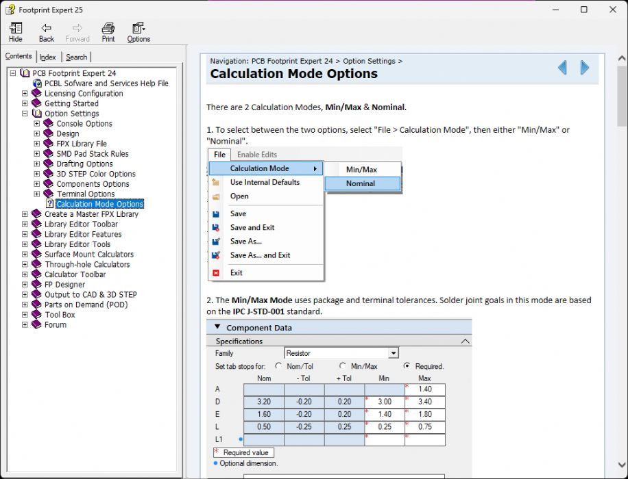 |
|
|
|
|
ulissescastro
Active User
Joined: 23 Feb 2022 Status: Offline Points: 18 |
Post Options
Thanks(0)
Quote Reply
Posted: 06 Jan 2025 at 4:34pm |
|
I think the problem is in the resolution and how many decimal points are used, please try to use at least 4 or 5 decimal points in your preferences. I do know is not realistic but please give it a try... Found the Fix, Thanks for helping...
by the way thanks for sharing the FED Vol 18 standard, for some reason I did came up to the same conclusions over the time... are you planning to give a quick update and presentation about it? I'm not sure if we can buy it or what its include on it. so a quick summary may help to justify it ;)
|
|
|
|
|
Tom H
Admin Group
Joined: 05 Jan 2012 Location: San Diego, CA Status: Offline Points: 5798 |
Post Options
Thanks(0)
Quote Reply
Posted: 06 Jan 2025 at 4:12pm |
|
I entered all your dimensions and concluded the same result.
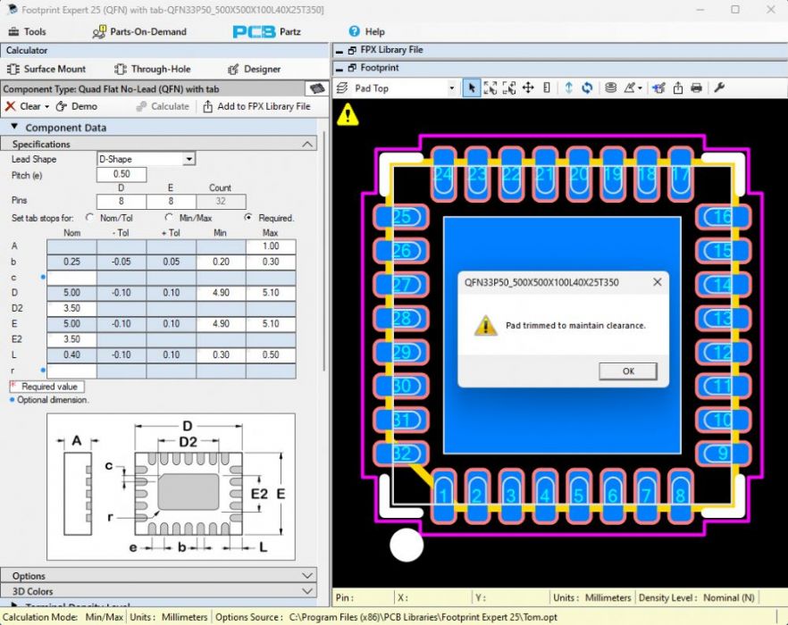
Footprint Expert is trimming the pads per the SMD Pad Stack Rules and turns off the Gang Mask feature.
 |
|
|
|
|
ulissescastro
Active User
Joined: 23 Feb 2022 Status: Offline Points: 18 |
Post Options
Thanks(0)
Quote Reply
Posted: 06 Jan 2025 at 4:00pm |
|
Fix it. it looks like the comparison should be >= instead or >... did a test and added 1 mil to the pad to pad and now it trims the leads and with no more gang mask...
|
|
|
|
|
ulissescastro
Active User
Joined: 23 Feb 2022 Status: Offline Points: 18 |
Post Options
Thanks(0)
Quote Reply
Posted: 06 Jan 2025 at 3:51pm |
|
Hi Tom, it looks to me that the gang feature is added before FPE compute the trimming.. Please try to replicate the following and these are my settings..
|
|
|
|
|
Tom H
Admin Group
Joined: 05 Jan 2012 Location: San Diego, CA Status: Offline Points: 5798 |
Post Options
Thanks(0)
Quote Reply
Posted: 06 Jan 2025 at 2:40pm |
|
You do not need to do 1:1 scale solder mask if you set the Minimum Pad to Pad Spacing to allow for a solder mask web.
What Solder Mask annular swell do you use? 0.05, 0.07 or 0.10? What is your Minimum Solder Mask Web? 0.07, 0.08 0.09 or 0.10? Multiply the Solder Mask annular swell by 2 and add the Minimum Solder Mask Web. Then use that value to set your Minimum Pad to Pad Spacing rule. This will effectively turn off the Gang Mask feature. |
|
|
|
|
ulissescastro
Active User
Joined: 23 Feb 2022 Status: Offline Points: 18 |
Post Options
Thanks(0)
Quote Reply
Posted: 06 Jan 2025 at 2:31pm |
|
I usually don't use the Altium solder mask Rule. in most cases it's useless. I do prefer to define the mask what Altium called "Manual" in my Footprints.
I do trust more in FPE than Altium, if the only solution now is to do 1:1 in FPE and then control it in the CAD tool, I do think this is going backwards, you should bring the option back.
What you describe at the end is what I was mentioning defining the pad to pad clearance. My question again is. Where can this feature be turned on or off or what is the value that will trigger FPE to to add the shape or not. is it the trimming of leads in your code preceding the mask feature or is it after? Thanks |
|
|
|
|
Post Reply
|
Page 12> |
| Tweet |
| Forum Jump | Forum Permissions You cannot post new topics in this forum You cannot reply to topics in this forum You cannot delete your posts in this forum You cannot edit your posts in this forum You cannot create polls in this forum You cannot vote in polls in this forum |


 Topic Options