

|
|
Via Fanout For BGA |
Post Reply 
|
| Author | |
mahmoodv99 
Advanced User 
Joined: 16 Jan 2016 Status: Offline Points: 93 |
 Post Options Post Options
") Thanks(0) Thanks(0)
 Quote Reply Quote Reply
 Topic: Via Fanout For BGA Topic: Via Fanout For BGAPosted: 10 May 2016 at 10:38pm |
|
Add option to add fan out for BGA in footprint itself with options via size, trace size, etc. 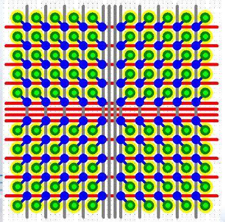
|
|
 |
|

|
|
|
|
|
Tom H
Admin Group 

Joined: 05 Jan 2012 Location: San Diego, CA Status: Offline Points: 6037 |
Post Options
Thanks(1)
Quote Reply
Posted: 15 May 2016 at 9:13am |
|
This feature is better to do in the CAD tool. Many CAD tools have automatic via fanout and if it doesn't, you need to ask the CAD vendor to add that feature into the CAD tool. Vias in a PCB Footprint library part become Pins and the BGA pad and via connecting line become Associated Copper. This makes the library part size very big. We tried this once and spent a lot of time creating it, but it was a disaster. It sounds like a good idea, but you should manually try to do it and put the resulting part in a PCB layout to test it. Then you will see that it's impossible to fanout BGA's in the library part. Also, most BGA's have unused pins and if those pins have vias, it blocks routing channels and bottom side capacitor placement. |
|
|
|
|
Post Reply
|
|
| Tweet |
| Forum Jump | Forum Permissions You cannot post new topics in this forum You cannot reply to topics in this forum You cannot delete your posts in this forum You cannot edit your posts in this forum You cannot create polls in this forum You cannot vote in polls in this forum |


 Topic Options