

|
|
Pad Stack Manager |
Post Reply 
|
Page 12> |
| Author | |
BennsPCB 
Advanced User 
Joined: 30 Jan 2013 Location: Sweden Status: Offline Points: 98 |
 Post Options Post Options
") Thanks(0) Thanks(0)
 Quote Reply Quote Reply
 Topic: Pad Stack Manager Topic: Pad Stack ManagerPosted: 03 Nov 2016 at 4:09am |
|
I'm creating a 4-pin SIP Hall sensor (Allegro A1363) FP and want to increase pad clearance by using an oblong pad instead of a round one, but Pad Stack Manager won't let me do that.
Why? Cheers, ... 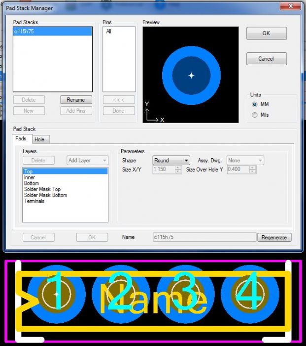 |
|
 |
|

|
|
|
|
|
Tom H
Admin Group 

Joined: 05 Jan 2012 Location: San Diego, CA Status: Offline Points: 6088 |
Post Options
Thanks(0)
Quote Reply
Posted: 03 Nov 2016 at 7:04am |
|
You Must create this part in FP Designer. The Calculator does not have a Oblong Through-hole pad stack option. |
|
|
|
|
BennsPCB
Advanced User
Joined: 30 Jan 2013 Location: Sweden Status: Offline Points: 98 |
Post Options
Thanks(0)
Quote Reply
Posted: 03 Nov 2016 at 7:21am |
|
OK Tom , I see. But, it seems like a 2-stage takeoff.
May I request a button that takes me to FP Designer directly (with the data already created)? And I still want to name it acc. to IPC-std. Perhaps with a note/naming that user defined padstack is used. Cheers, ... |
|
|
|
|
Tom H
Admin Group
Joined: 05 Jan 2012 Location: San Diego, CA Status: Offline Points: 6088 |
Post Options
Thanks(0)
Quote Reply
Posted: 03 Nov 2016 at 7:29am |
|
There is a button to move your Calculator part to FP Designer. However, these component families will not transfer - DPAK, TO220, TO92, Mounting Holes, Aluminum
Electrolytic Capacitor. 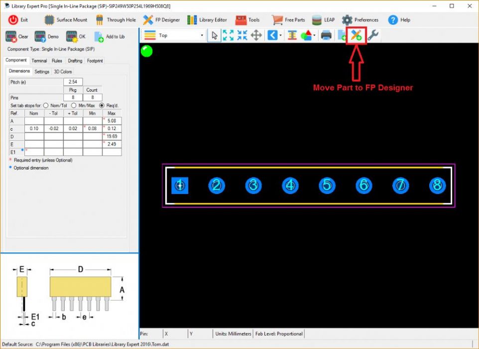 |
|
|
|
|
BennsPCB
Advanced User
Joined: 30 Jan 2013 Location: Sweden Status: Offline Points: 98 |
Post Options
Thanks(0)
Quote Reply
Posted: 03 Nov 2016 at 7:37am |
|
Tried that, but all data except the pins disappeared. Not very useful.
|
|
|
|
|
Tom H
Admin Group
Joined: 05 Jan 2012 Location: San Diego, CA Status: Offline Points: 6088 |
Post Options
Thanks(0)
Quote Reply
Posted: 03 Nov 2016 at 7:43am |
|
Did you select the "Body" tab and enter the package dimensions? 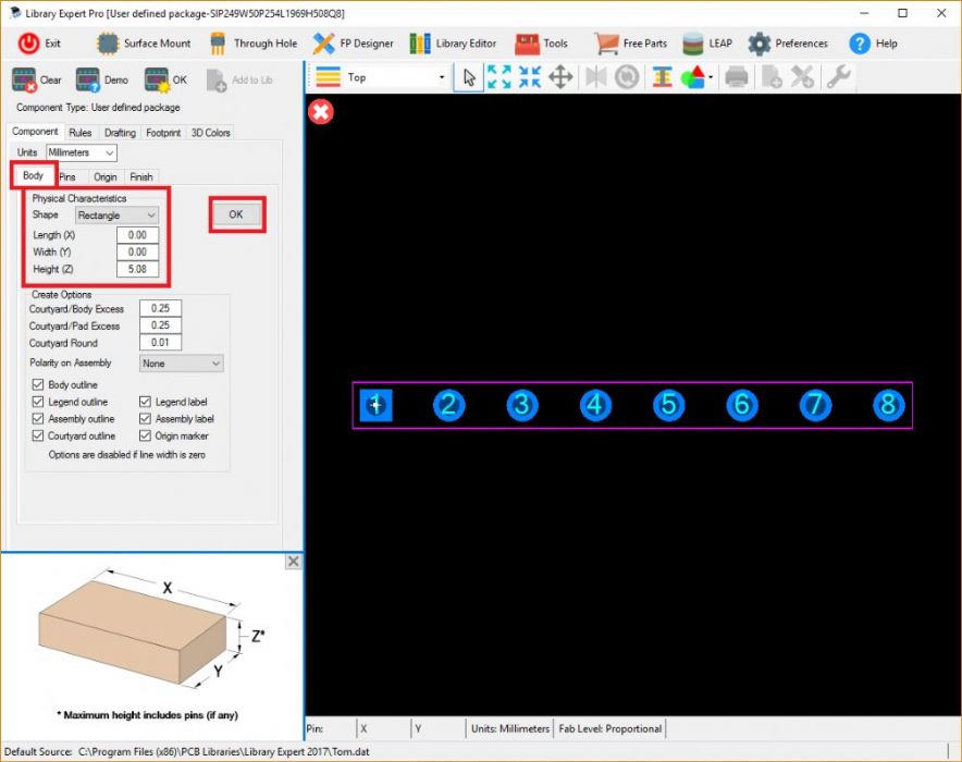 |
|
|
|
|
BennsPCB
Advanced User
Joined: 30 Jan 2013 Location: Sweden Status: Offline Points: 98 |
Post Options
Thanks(0)
Quote Reply
Posted: 03 Nov 2016 at 8:21am |
|
Nope, I came from Through Hole/Single In-Line Package (SIP), where I have entered all my data.
It's from here it would be useful to enter the FP Designer. (with data intact)  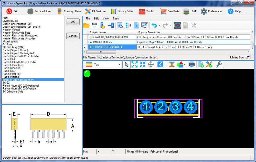 |
|
|
|
|
Tom H
Admin Group
Joined: 05 Jan 2012 Location: San Diego, CA Status: Offline Points: 6088 |
Post Options
Thanks(0)
Quote Reply
Posted: 03 Nov 2016 at 8:38am |
|
OK, this is a bug and we're going to release V2016.14 later today. In the meantime, you can create that 4-pin SIP in FP Designer with Oblong PTH pad stacks in less than 3 minutes. Thank you for reporting this issue. |
|
|
|
|
BennsPCB
Advanced User
Joined: 30 Jan 2013 Location: Sweden Status: Offline Points: 98 |
Post Options
Thanks(0)
Quote Reply
Posted: 03 Nov 2016 at 8:47am |
|
OK, nice
 Cheers, ... |
|
|
|
|
Nick B
Admin Group

Joined: 02 Jan 2012 Status: Offline Points: 2020 |
Post Options
Thanks(0)
Quote Reply
Posted: 03 Nov 2016 at 4:27pm |
|
2016.14 is online in our Downloads section, please run it and let us know.
|
|
|
|
|
Post Reply
|
Page 12> |
| Tweet |
| Forum Jump | Forum Permissions You cannot post new topics in this forum You cannot reply to topics in this forum You cannot delete your posts in this forum You cannot edit your posts in this forum You cannot create polls in this forum You cannot vote in polls in this forum |


 Topic Options