

|
|
Error with Footprint Designer and OrCAD PCB |
Post Reply 
|
Page 12> |
| Author | |
Lekselius 
New User 

Joined: 10 Apr 2013 Location: Sverige Status: Offline Points: 21 |
 Post Options Post Options
") Thanks(1) Thanks(1)
 Quote Reply Quote Reply
 Topic: Error with Footprint Designer and OrCAD PCB Topic: Error with Footprint Designer and OrCAD PCBPosted: 04 Jun 2013 at 6:58am |
|
When generating an Ethernet connector for OrCAD PCB V16.6 using "FP Designer" (FD) the pads are wrong. They look OK in "Footprint Designer" but there is an error when running the .bat file and the resuling footprint are without holes.
I have tried this both with OrCAD V16.3 and OrCAD V16.6 with the same result.
The error message from the padstack editor is: --- PADSTACK
ERRORS and WARNINGS:
DEFAULT
INTERNAL: No pads are defined. When loaded into a design, no internal pads
will be added for unmatched padstack layers or when
additional internal connection layers are added to the design. Drill hole
size is equal or larger than smallest pad size. --- The large mechanical hole are incorrect in the resulting footprint and all holes are missing drill information etc. Attached are screenshot of the error message, FP designer window with the footprint, and the resulting footprint in Orcad PCB designer 16.3. Attached are also the exported footprint to be run with orcad 16.6. 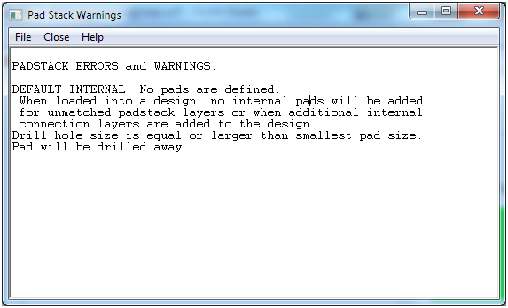 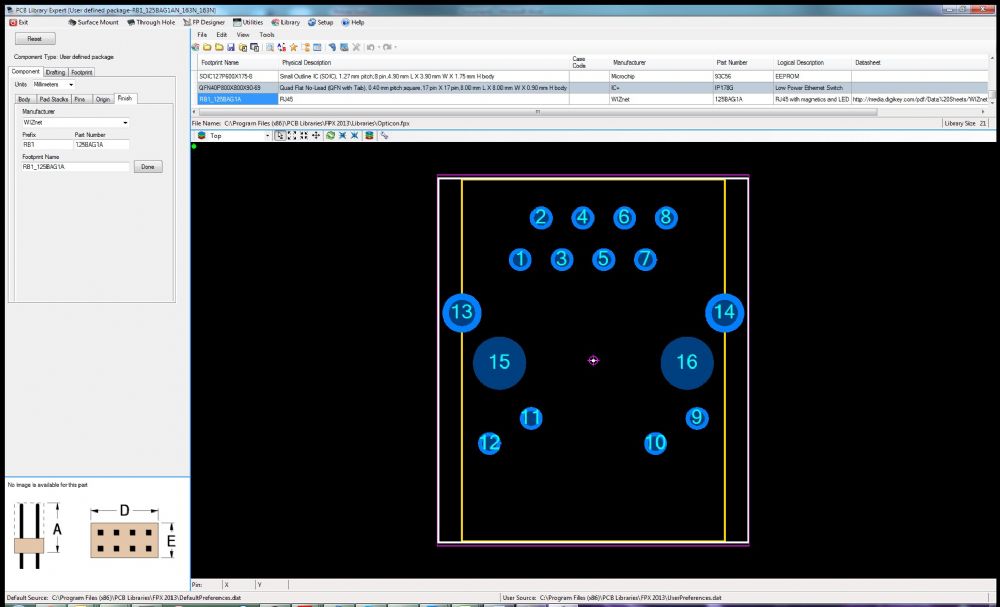 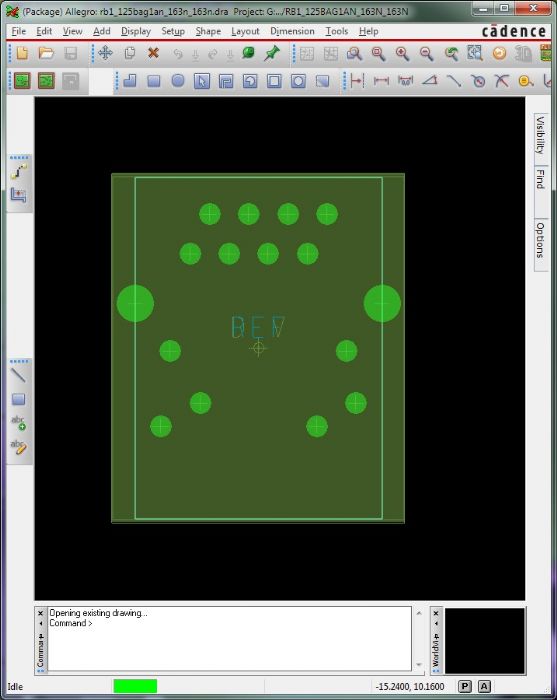 |
|
 |
|

|
|
|
|
|
chrisa_pcb
Moderator Group 

Joined: 29 Jul 2012 Location: San Diego Status: Offline Points: 772 |
Post Options
Thanks(1)
Quote Reply
Posted: 05 Jun 2013 at 3:08pm |
|
Hi,
What version of our tool are you currently using?
|
|
|
|
|
Lekselius
New User
Joined: 10 Apr 2013 Location: Sverige Status: Offline Points: 21 |
Post Options
Thanks(1)
Quote Reply
Posted: 06 Jun 2013 at 11:23pm |
|
I'm running PCB Library Expert version 2013.02
|
|
|
|
|
Tom H
Admin Group

Joined: 05 Jan 2012 Location: San Diego, CA Status: Offline Points: 6069 |
Post Options
Thanks(1)
Quote Reply
Posted: 07 Jun 2013 at 7:03am |
|
Did you watch this Footprint Designer training video?
http://www.pcblibraries.com/products/fpx/userguide/default.asp?ch=104 http://www.pcblibraries.com/forum/pcb-library-construction-guidelines_forum30.html |
|
|
|
|
Lekselius
New User
Joined: 10 Apr 2013 Location: Sverige Status: Offline Points: 21 |
Post Options
Thanks(1)
Quote Reply
Posted: 11 Jun 2013 at 10:57pm |
|
I have watched the video and followed the exact same step as in the tutorial, creating an identical footprint but I get the same error when importing the footprint as I got previously.
This is the footprint in package designer:  Error when running the batch file:  Resulting footprint in Orcad:  And the files to create the Orcad footprint created by FP designer: Tutorial_1234N.zip |
|
|
|
|
BennsPCB
Advanced User 
Joined: 30 Jan 2013 Location: Sweden Status: Offline Points: 98 |
Post Options
Thanks(1)
Quote Reply
Posted: 15 Jun 2013 at 7:27am |
|
Have you turned on "Setup/Design Parameters.../Display non-plated holes".
Otherwise you only see the pad, which will be drilled away. Just my 2 cents, ... |
|
|
|
|
d_nilsson
New User
Joined: 22 Jul 2013 Location: Sweden Status: Offline Points: 12 |
Post Options
Thanks(1)
Quote Reply
Posted: 25 Jul 2013 at 4:55pm |
|
Hi,
Was this issue ever resolved? I'm running into the same problem, using FP Designer in version 2013.08. If I open up the sample part AMPH_10-507143-85E in Sample Data - FP Designer.fpx and try to just build it (no changes) for Orcad PCB 16.6 the padstack definition for the NPTHs (keying holes using padstack c100hn295k395_395) is invalid. Cadence padstack editor will spit out during processing of the batch file: PADSTACK ERRORS and WARNINGS: Drill hole size is equal or larger than smallest pad size. Pad will be drilled away. I think this is since what FP Designer is telling Cadence to do is to add 1mm pads on all layers without thermal relief or anti-pad and then drill with a 2.95mm drill, Cadence doesn't like that definition of a NPTH. Is this a known bug? Any workarounds? According to padstack designer in FP Designer there should be a 3.95mm antipad, but that antipad seems to be set to "null" in Cadence when instead it maybe should have been the regular pad that should have been set to "null". Thanks Daniel |
|
|
|
|
Tom H
Admin Group
Joined: 05 Jan 2012 Location: San Diego, CA Status: Offline Points: 6069 |
Post Options
Thanks(1)
Quote Reply
Posted: 25 Jul 2013 at 5:41pm |
|
The CAD interface programmer (Chris) is on vacation and will be back next week. |
|
|
|
|
d_nilsson
New User
Joined: 22 Jul 2013 Location: Sweden Status: Offline Points: 12 |
Post Options
Thanks(0)
Quote Reply
Posted: 26 Jul 2013 at 4:12am |
|
Ok, I will manually modify the padstack definition in Orcad PCB Designer then until Chris is back.
|
|
|
|
|
chrisa_pcb
Moderator Group
Joined: 29 Jul 2012 Location: San Diego Status: Offline Points: 772 |
Post Options
Thanks(1)
Quote Reply
Posted: 10 Aug 2013 at 12:44pm |
|
I'll be looking at fixing this issue shortly, but it probably won't make it into the tool until the next update in a couple of weeks.
|
|
|
|
|
Post Reply
|
Page 12> |
| Tweet |
| Forum Jump | Forum Permissions You cannot post new topics in this forum You cannot reply to topics in this forum You cannot delete your posts in this forum You cannot edit your posts in this forum You cannot create polls in this forum You cannot vote in polls in this forum |


 Topic Options