|
|
How To Specify Plated Holes? |
Post Reply 
|
Page 12> |
| Author | |
Aerolink 
Active User 

Joined: 26 Feb 2014 Status: Offline Points: 45 |
 Post Options Post Options
") Thanks(0) Thanks(0)
 Quote Reply Quote Reply
 Topic: How To Specify Plated Holes? Topic: How To Specify Plated Holes?Posted: 28 Aug 2014 at 8:52am |
|
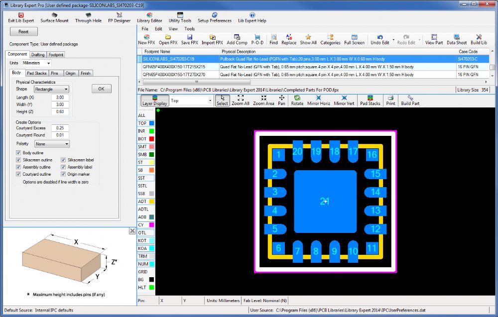
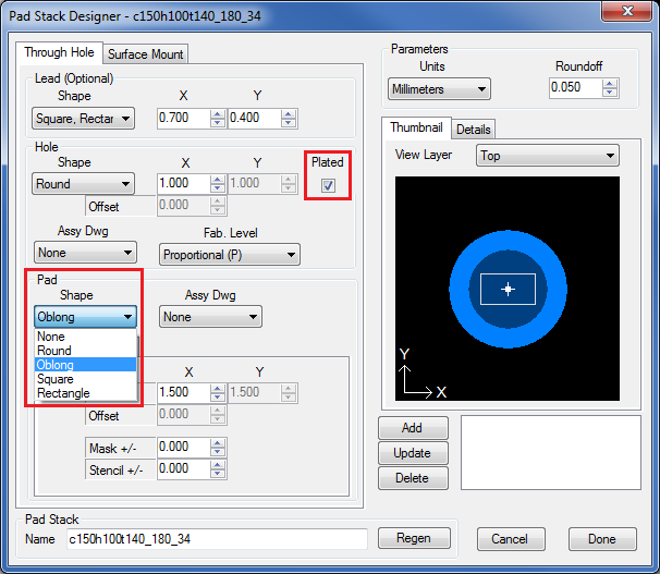
How do I specify that my pin holes are to be plated? I see there is a checkbox that say's "Plated" when I view the pad stack. The box is checked and greyed-out but my boards came back with unplated holes. Did I miss something? |
|
 |
|

|
|
|
|
|
Tom H
Admin Group 

Joined: 05 Jan 2012 Location: San Diego, CA Status: Offline Points: 6075 |
Post Options
Thanks(0)
Quote Reply
Posted: 28 Aug 2014 at 9:06am |
|
We need to know if you are referring to the IPC Calculator or FP Designer. We also need to know what version of Library Expert are you using? V2014.08 is the latest release with updates to the FP Designer Pad Stack Manager. |
|
|
|
|
Aerolink
Active User
Joined: 26 Feb 2014 Status: Offline Points: 45 |
Post Options
Thanks(0)
Quote Reply
Posted: 29 Aug 2014 at 7:55am |
|
V2013.20 FP Designer
|
|
|
|
|
Tom H
Admin Group
Joined: 05 Jan 2012 Location: San Diego, CA Status: Offline Points: 6075 |
Post Options
Thanks(0)
Quote Reply
Posted: 29 Aug 2014 at 8:07am |
|
You should download V2013.21. That will help.
I haven't used V2013 since last February and FP Designer has a completely new Pad Stack Manager in the current V2014.08.
|
|
|
|
|
ernestorey
New User 
Joined: 10 Apr 2014 Location: Santa Clara, CA Status: Offline Points: 10 |
Post Options
Thanks(0)
Quote Reply
Posted: 29 Aug 2014 at 1:50pm |
|
You should always review your GERBER files prior to sending them out, use an independent GERBER viewer (not tied to the layout tool) to check the outputs. I recommend ViewMate from www.pentalogix.com, been using it for 10+ years.
Regarding your holes, if drilled through a metal pad they will be plated. If there is no metal on the outer layers they will be unplated. If the metal is the same size as the finished hole size, they will be unplated since they need to be drilled larger in order to plate.
On many drill data outputs the plated/not-plated information is not encoded in the NC files, you should have a drill "map" or "chart" as part of the GERBERs or the Fabrication Drawing specifying which holes you want plated or unplated.
|
|
|
|
|
Aerolink
Active User
Joined: 26 Feb 2014 Status: Offline Points: 45 |
Post Options
Thanks(0)
Quote Reply
Posted: 31 Aug 2014 at 9:52am |
|
Unfortunately, when using SoloPCB for layout, we are not given access to our Gerbers until after the board is purchased! This has caused a lot of trouble for me and after one round of bad boards I convinced my vendor (Mass Design) to share the files with me. I spotted that problem right away.
Unfotunately, round two has this thru-hole plating problem. I need to figure this out before round three. BTW, I use the same viewer as you,,, when I have files to view. Anyway, back to the problem. On EVERY thru-hole component I have created, my actual boards come back without plated holes. Every hole that is to be connected to a power or ground plane is not connected due to lack of plating. The gerbers look correct. They show thermal reliefs to the pin hole when I view the plane layers. There are no top or bottom layer signals to these pins but the pad rings look normal and are plated, just not the bores. You may be onto the problem with the hole sizes versus drill sizes. I don't know the mfg process, but could they have drilled out the plating? All I find related to this is the greyed out, but checked, "Plated" checkbox on the padstack manager. Not sure why it is greyed out, but at least it is checked. The pad size is 2.20 and hole is 1.6, so I don't see a problem there. I just want to understand how this works from the library point of view to see if I missed something when I created these footprints. I will post to the SoloPCB forum too. I hate to think this is a problem with the PCB Library version I am using?!?! Certainly someone else would have run across this by now? |
|
|
|
|
Aerolink
Active User
Joined: 26 Feb 2014 Status: Offline Points: 45 |
Post Options
Thanks(0)
Quote Reply
Posted: 31 Aug 2014 at 9:55am |
|
Is there any reason why I shouldn't just upgrade to 2014-08? You suggested a 2013 version.
|
|
|
|
|
Tom H
Admin Group
Joined: 05 Jan 2012 Location: San Diego, CA Status: Offline Points: 6075 |
Post Options
Thanks(0)
Quote Reply
Posted: 31 Aug 2014 at 10:07am |
|
You should upgrade to V2014.09 which will be available next week -
|
|
|
|
|
Aerolink
Active User
Joined: 26 Feb 2014 Status: Offline Points: 45 |
Post Options
Thanks(0)
Quote Reply
Posted: 31 Aug 2014 at 11:44am |
|
Will do...
Does the footprint convey plated versus non-plated holes to the layout tools or not? As I look into this further, I find nothing in the footprint that would indicate that holes are NOT to be plated. The "Plated" checkbox seems always to be checked, as I would expect for a thru-hole part. I just reviewed my drill layer in SoloPCB and sure nuf, the drill chart says "Non-Plated" for all of the holes related to my footprints. I can use the SoloPCB's padstack editor to mark these holes as plated (clearing the "Non-Plated" checkbox) and all looks well again.... So.... where did this fall apart? Does the footprint convey platedness to the layout tools? If so, then the layout tool is not honoring this info. If the footprint does NOT convey plated info, then it would appear to be human error (me of course) for not knowing enough to edit the padstacks that need plating (seems like a sensible "default" for thru-hole parts to me). |
|
|
|
|
Tom H
Admin Group
Joined: 05 Jan 2012 Location: San Diego, CA Status: Offline Points: 6075 |
Post Options
Thanks(0)
Quote Reply
Posted: 31 Aug 2014 at 12:52pm |
|
In the through-hole Calculator component families, every hole is automatically plated and you have no control of that with the exception of the Mounting Hole calculator can toggle Plated or Non-plated. The FP Designer the user has a Plated check box and an assortment of pad shapes. And even though the calculator will provide a good annular ring, the user can override the calculation and enter a unique pad size.
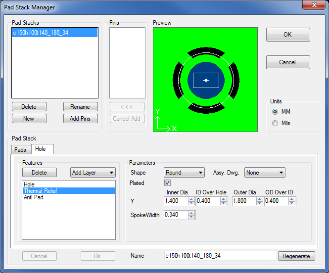
Once the pad stacks are created and you select the "Done" button, the Pad Stack Manager dialog window will open. That allows the user to further customize each pad stack for outer and inner layers, solder and paste mask, anti-pad and thermal relief, making the FP Designer totally flexible to create unique pad stacks.
|
|
|
|
|
Post Reply
|
Page 12> |
| Tweet |
| Forum Jump | Forum Permissions You cannot post new topics in this forum You cannot reply to topics in this forum You cannot delete your posts in this forum You cannot edit your posts in this forum You cannot create polls in this forum You cannot vote in polls in this forum |


 Topic Options