Mfr Recommended, Tolerances & Affected Pad Stacks
Printed From: PCB Libraries Forum
Category: PCB Footprint Expert
Forum Name: Questions & Answers
Forum Description: issues and technical support
URL: https://www.PCBLibraries.com/forum/forum_posts.asp?TID=3699
Printed Date: 28 Aug 2026 at 3:39am
Topic: Mfr Recommended, Tolerances & Affected Pad Stacks
Posted By: Nick B
Subject: Mfr Recommended, Tolerances & Affected Pad Stacks
Date Posted: 28 Aug 2026 at 1:34am
|
QUESTION:
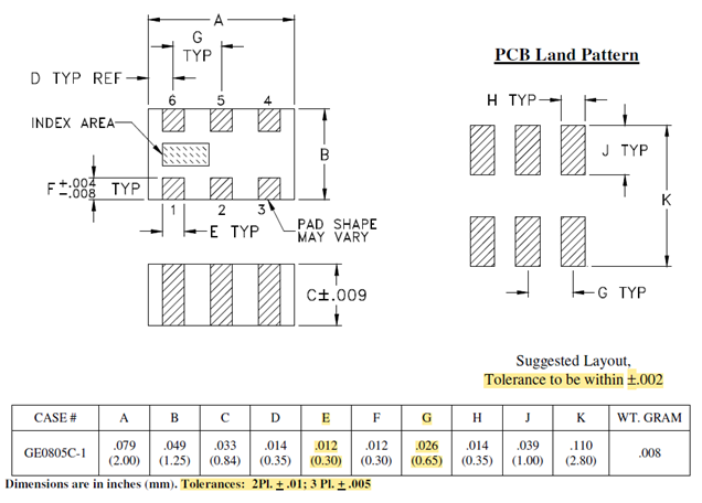
ANSWER: Manufacturer package tolerances are mostly too robust and not reality. They don't realize that their tolerances impact pad stack calculations and all the drafting outlines that are mapped to the maximum material condition. Any package with dimensions like a 0805 package should have a realistic maximum tolerance of 0.15 mm max, 0.10 mm nom. or 0.05 mm minimum. We prefer to use the minimum tolerance of 0.05 because it's realistic. It’s the goal of every component manufacturer to create packages near the Nominal Package Dimensions and their recommended patterns prove that. 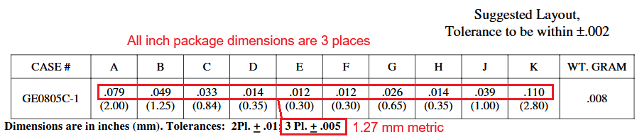 The Mini-Circuits Recommended Pattern does not accommodate their package in the Minimum or Maximum material condition for the tolerances they provide. i.e.: if you used the manufacturer package dimensions in the minimum or maximum tolerances, would they fit on the pattern? Here is the Mini-Circuits Recommended Pattern using their negative tolerance. Pad stacks are too way robust for their minimum material condition. 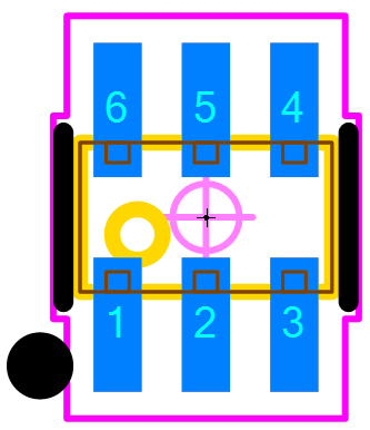 Here is the Mini-Circuits Recommended Pattern using their positive tolerance. Not sufficient pad stack for maximum material condition. 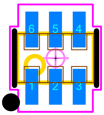 Here is the Mini-Circuits Recommended Pattern using no tolerances. Perfect pattern for a package using no tolerances. 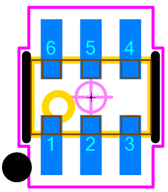 It looks like Mini-Circuits did not use their own tolerances when they created their Recommended Pattern. Component manufacturers need to make their package tolerances realistic. They should measure the packages coming off the manufacturing line to print the real package tolerances in the datasheets. Don't make up fictious tolerances that don’t match reality. ------------- Stay connected - follow us! https://twitter.com/PCBLibraries" rel="nofollow - X - http://www.linkedin.com/company/pcb-libraries-inc-/" rel="nofollow - LinkedIn |
 MINI-CIRCUITS has a wide range of RF devices with non-JEDEC/custom package types, e.g. the selected DLFCG-540+ (Case GE0805C-1) 6-pin SMT ceramic filter.