Package and Terminal Tolerances
Printed From: PCB Libraries Forum
Category: Libraries
Forum Name: PCB Libraries Guideline
Forum Description: (online edition)
URL: https://www.PCBLibraries.com/forum/forum_posts.asp?TID=3693
Printed Date: 12 Oct 2026 at 5:15pm
Topic: Package and Terminal Tolerances
Posted By: Nick B
Subject: Package and Terminal Tolerances
Date Posted: 20 Aug 2026 at 11:00am
|
Component and Terminal tolerances affect the resulting pad stack size and spacing. Many component manufacturer package and terminal tolerances are too robust and unrealistic. Especially in component datasheets that are 20 - 30 years old. The machines that produce today's component packages are fairly accurate and it's the manufacturers' goal to produce component packages in the Nominal Material Condition. The IPC-7352 mathematical model is 100% dependent on package tolerances to form the solder joint goals for assembly attachment to accommodate the package in all 3 material conditions for Least, Nominal and Most. PCB component package tolerances account for variations in manufactured electronic component dimensions, ensuring that physical parts safely fit on their designated circuit board footprints. Every electronic component has minor sizing variations due to material changes, tooling wear, and thermal expansion during assembly. Circuit designers must accommodate these variations when building CAD libraries to prevent assembly failures, bad solder joints, or physical placement collisions. When a semiconductor component manufacturer datasheet with package dimensions only provides Nominal dimensions for the Body Length and Width the PCB librarian must assign a 0.10 mm minimum, 0.15 mm nominal or 0.20 mm maximum tolerance. Terminal Tolerances vary. But the range averages between 0.10 and 0.20, same as package tolerances.
IPC-7351B refers to a mathematical model that also includes Fabrication and Assembly tolerances. IPC-7352 does not consider these tolerances. The mathematical model takes into consideration the minimum and maximum package and terminal dimensions to ensure that the resulting footprint accommodates the package tolerance range. Tolerances are referred to as Min/Max technology. This means the pad stack size and spacing will accommodate the component package in the minimum or maximum material condition. Since the package and terminal tolerances affect the resulting pad stack size and spacing, robust tolerances will produce larger pad stacks while no tolerances will produce pad stacks that are too small. The IPC-7351 Side solder joint goal for chip packages is zero. The pad width is the same dimension as the Maximum terminal lead width. When the Heel Solder Joint Goal for chip packages is zero, the heel goal is determined by the terminal lead and package length tolerances. The Toe normally has a solder joint goal has a predefined value. Then the terminal lead and package length tolerances are added to the Toe value. The resulting Toe solder joint is a combination of the Toe goal value and terminal and package length tolerances. The goal is to have one Case Code footprint for every resistor in your supply chain. If you have 10 resistor suppliers and they provide different tolerances, to achieve this goal, standard tolerances that can accommodate all 10 vendors packages must be documented. Because every component family has a unique 3D STEP model, it's necessary to create a footprint for each component family. Inductor, Resistor, Capacitor, Diode, etc. all have unique 3D STEP models. Recommended Package tolerances for chip case codes:
Different component manufacturers will publish a wide range of tolerances. For example, Panasonic, Yageo, Vishay, AVX, Murata, Kemet and Taiyo Yuden will have different tolerances to the same Case Code. But the PCB designer or CAD librarian want one set of tolerances for each Case Code. Here is a 0603 Chip with no tolerances:  Here is a 0603 Chip with a 0.05 tolerance on Length, Width and Terminal Nominal Density Level:  Here is a 0603 Chip with a 0.10 tolerance on Length, Width and Terminal Nominal Density Level. This is the optimal footprint pattern.  Here is a 0603 Chip with a 0.15 tolerance on Length, Width and Terminal Nominal Density Level, Slightly robust. 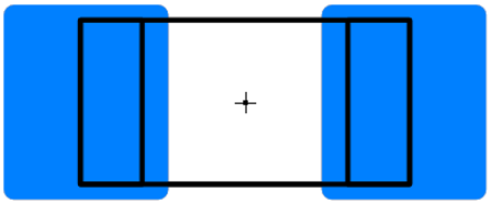 Here is a 0603 Chip with a 0.20 tolerance on Length, Width and Terminal Nominal Density Level. Too robust. 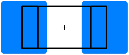 Here is a 0603 Chip with a 0.25 tolerance on Length, Width and Terminal Nominal Density Level. Grossly robust. 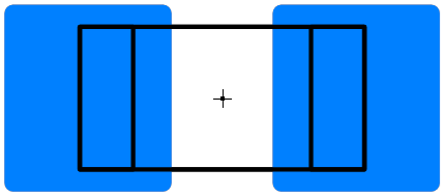 Here is a 0603 Chip with a 0.10 tolerance on Length, Width and Terminal for IPC Least Density Level:  Here is a 0603 Chip with a 0.10 tolerance on Length, Width and Terminal for IPC Most Density Level:  Chip component manufacturers do not use their package tolerances when publishing their manufacturer recommended patterns in their datasheets. They use nominal package dimensions and add a Toe, Heel and Side solder joint regardless of how robust their tolerances are. If component tolerances are real and component packages can be shipped to assembly shops and some come in the minimum material condition and some come in the maximum material condition, there will be assembly attachment issues. Beware of component manufacturers recommended solder patterns. Make sure they can accommodate the tolerances provided in their datasheet. In the future, component package tolerances will be very small and even nonexistent. When this happens, the IPC-7352 Mathematical Min/Max model becomes obsolete. When component packages are produced without tolerance, a new model for calculating pad stacks must replace the IPC-7352 math. The Nominal calculation mode only requires nominal component package dimensions and solder joint goals for Toe, Heel and Side. Currently, many IPC-7352 Heel and Side solder joint goals are 0.00 and the Heel and Side goals rely 100% on package tolerances. When package tolerances are 0.00 the solder joint goals for Heel and Side must be updated to values that are consistent across all terminal lead forms. 
 The Footprint Expert automates footprints to perfection. Professional, detailed, and accurate parts - all built consistently with identical rules, regardless of how many people are involved in your library development. Get your FREE Footprint Calculator or Footprint Expert Evaluation License: https://www.pcblibraries.com/Register" target="_blank rel="nofollow" - https://www.PCBLibraries.com/Register Call us - 847-557-2300 ------------- Stay connected - follow us! https://twitter.com/PCBLibraries" rel="nofollow - X - http://www.linkedin.com/company/pcb-libraries-inc-/" rel="nofollow - LinkedIn |