Drafting Outlines & Polarity Marking
Printed From: PCB Libraries Forum
Category: Libraries
Forum Name: PCB Libraries Guideline
Forum Description: (online edition)
URL: https://www.PCBLibraries.com/forum/forum_posts.asp?TID=3692
Printed Date: 29 Aug 2026 at 3:43am
Topic: Drafting Outlines & Polarity Marking
Posted By: Nick B
Subject: Drafting Outlines & Polarity Marking
Date Posted: 20 Aug 2026 at 11:00am
|
Overview PCB drafting outlines and polarity markings are critical for preventing component failure, rework, and assembly errors. Proper drafting requires clear component boundaries (silkscreen outlines), exact Pin-1 markers for ICs, and unambiguous anode/cathode (or positive/negative) indications for polarized devices. Silkscreen Drafting Options 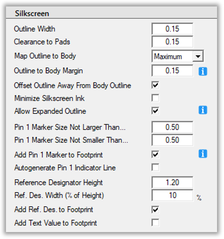 General: Silkscreen is a non-conductive ink layer applied to provide visual guidance for assembly, testing, and maintenance. Outline Width: default settings can be changed to your company standard. Fabrication minimum silkscreen line width is 0.10. The nominal line width is 0.15 and maximum line width is 0.20 (but any value above 0.10 is acceptable). Clearance to Pads: Defines the minimum allowable space between calculated silkscreen outlines and adjacent pads or applied to clearance between silkscreen articles. To avoid this violation lines may be terminated or trimmed. Polarity indicator placement may be adjusted. 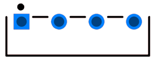 Map Outline to Body: This drop-down menu sets the size of the silkscreen outline relative to the component body. The "Margin" option is applied in conjunction with the Outline to Body option. The default value is "Maximum". 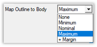 Outline To Body Margin: Defines the silkscreen outline-to-nominal body spacing when "+Margin" is selected. Offset Outline away from Body Outline: When checked, the silkscreen size is offset by an additional ½ line width to minimize the chance of obscuration by a component body. 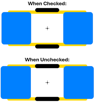 Minimize Silkscreen Ink: When this option is checked, the Grid Array silkscreen outlines will be hatched. When it is unchecked, the silkscreen outline will be a full body outline. 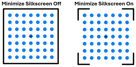 Allow Expanded Outline: Allows expansion as required in order to add an outline to micro-miniature parts. Error message when Expanded Outline Off: 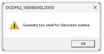 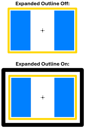 Pin 1 Markers General: Markers are only added to parts having a polarity. For example, Diodes and polarized capacitors may have polarity, resistors and inductors do not have polarity and can be inverted during assembly. Pin 1 Marker Size Not Larger/Not Smaller Than: The silkscreen polarity dot size is automatically calculated to adjust to the component while maintaining a size within the range of these two values. Making the values equal results in a fixed dot size. Add Pin 1 Marker to Footprint: Enables or disables the automatic addition of polarity dot markers. Silkscreen polarity markers are placed to conform to the drafting settings and component physical constraints. If the automatic placement is found to be unacceptable, you can manually add Polarity Symbols. 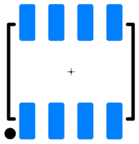 When the pads are too short or under the package, a pin 1 dot at the end of the pad is acceptable. 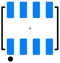 Autogenerate Pin 1 Indicator Line: Enables the addition of a line next to pin1 on some parts, typically ICs. 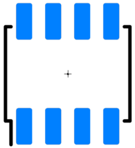 Reference Designator Height and Width: Fonts are not an option owing to differences in CAD translator options, so FPE uses height as a dimension with a percentage of height defining pen width. The effect of width can't be observed in FPE. Add Reference Designator to Footprint: Enables or disables the Reference Designator for a translated output. Add Value to Footprint: Enables or disables an additional silkscreen text "Value" for a translated output. Assembly Drafting Options 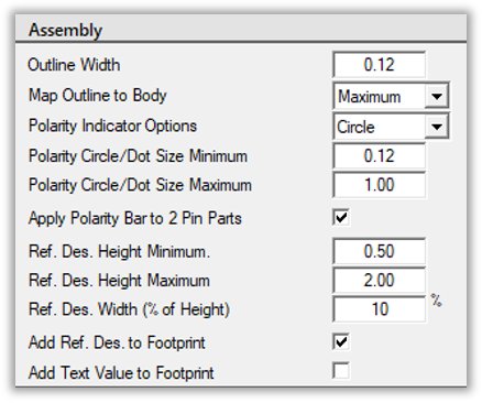 General: Assembly layer drafting elements provide visual and dimensional details that guide component placement, orientation, and verification. Assembly layers and are critical for manufacturing accuracy. Outline Width: The assembly outline never gets manufactured, so the line width is user definable. Map Outline to Body: This drop-down menu sets the size of the silkscreen outline relative to the component body. The default value is "Maximum". Polarity Indicator Options 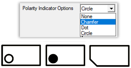 Pin 1 Dot/Circle Size Not Larger/Not Smaller Than: The silkscreen polarity dot size is automatically calculated to adjust to the component while maintaining a size within the range of these two values. Making the values equal results in a fixed dot size. The Chamfer also automatically adjusts the component size to maintain a size within the range of 1/3 the lesser of body height or width, not to exceed 1 millimeter. Add Polarity Bar To 2 Pin Parts: When checked, polarity Indicator options are replaced by wide line at the pin 1 location of polarized 2 pin parts.  Reference Designator Height Minimum and Maximum: Text values are automatically calculated to fit within the assembly outline while maintaining a size within the range of these two values. Making the values equal results in a fixed dot size. Fonts are not an option owing to differences in CAD translator options, so FPE uses height as a dimension with a percentage of height defining pen width. The effect of width can't be observed in FPE. Add Reference Designator to Footprint: Enables or disables the Reference Designator for a translated output. Add Value to Footprint: Enables or disables an additional assembly text "Value" for a translated output. Courtyard Options 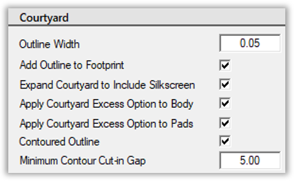 General: A courtyard defines the minimum clearance area around a component's footprint to ensure manufacturability, assembly, and rework-ability. It is not part of any electrical circuit but is critical for mechanical and process requirements. The courtyard to body is mapped to the maximum package dimensions. Outline Width: User definable. Add Outline to Footprint: Enables or disables addition of the Courtyard to the footprint. Expand Courtyard to Include Silkscreen: Allows expansion of the Courtyard to encompass the Silkscreen outline in situations where the Silkscreen size exceeds the Courtyard. 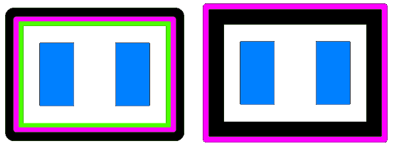 Apply Courtyard Excess to Body/Pads: When checked, does not add the excess over body, or pads respectively, to courtyard. Note: The Expand Courtyard to Include Silkscreen is not affected by this option. Courtyard Excess values: These values are not found in the Courtyard Drafting Options but are included with Terminal Options and, as such, unique to each terminal type - grid arrays, surface mount and thru-hole. Contoured Courtyard: When checked, allows the Courtyard to conform to irregular shapes that might be present in the footprint. 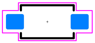 Rectangular Courtyard: This was the original IPC-SM-782 courtyard shape. 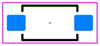 Minimum Cut in Gap: This option defines the minimum size of a space that can included by a Courtyard contour. Values smaller than this size will be ignored by the contour. 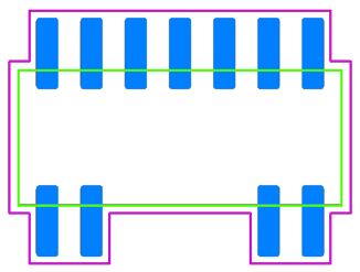 Origin Options 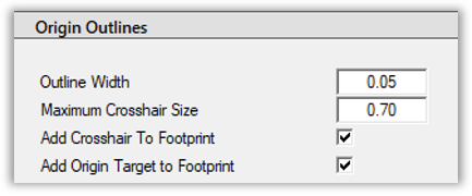 General: An Origin construct defines a visual, physical reference indicating a point from which all other footprint dimensions may be referenced. The Origin construct consists of two independent drafting features forming a crosshair and circle. Outline Width: user definable as there is no industry standard. Maximum Crosshair Size: defines the maximum length of a crosshair line (plus the outline width). As a footprint shrinks, the crosshair size is reduced in proportion to the courtyard. Add Crosshair to Footprint: When checked allows an origin crosshair to be added to a footprint. Add Target to Footprint: When checked allows an origin target to be added to a footprint. Component and Terminal Options 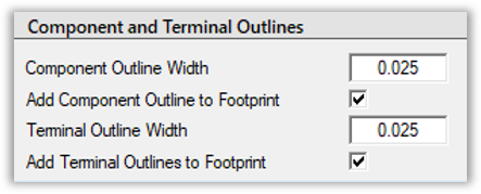 General: Component and terminal outlines are always shown in the nominal material condition. This is done to maintain a consistent relationship that prevents confusing overlapping outlines that would occur with mixed material conditions. Component Outline Width: User definable. Add To Footprint: When checked, allows the nominal component body outline to be added to a footprint. Terminal Outline Width: User definable. This feature is used for visibility of the terminal lead on the pad. If the terminal lead is not 100% on the pad, there is something wrong with the dimensions. Add To Footprint: When checked, the nominal terminal outlines to be added to the footprint. Drafting Element Properties General: Right-clicking on any of the drafting items will open a dialog box, appropriate to the selected item, displaying its characteristics for viewing only. 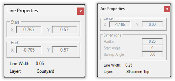 Symbol and Keep-out Creation Tools The Symbol and Keep-out Creation Tools provide the means for manual design and placement of drafting elements that do not lend themselves to an automatic Calculator function. The tools are activated from a drop-down button on the Footprint Viewer toolbar. 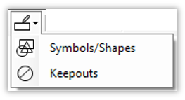 Symbol/Shapes and Keep-outs: Clicking either drop-down item Opens the Symbol Shape or Keep-out Properties Dialog Boxes respectively. Note: Adding drafting symbols should be done as a final step in footprint creation. Symbols and keep-outs are typically placed in relation to other footprint features. Therefore, any time a component specification, rule or drafting element is changed, all manually added symbols and Keep-outs are deleted. However, once added, symbols and keep-outs are saved to the FPX library with the footprint. Drafting Symbol Creation 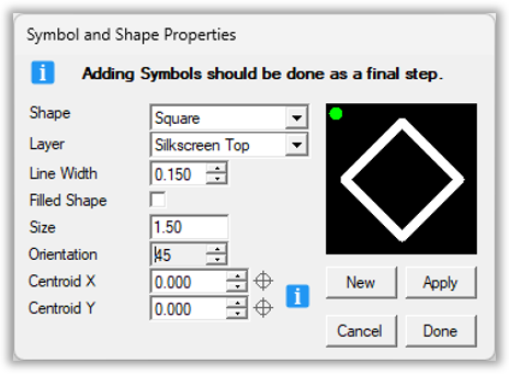 Shape: The following illustrates a variety of available symbol shapes. Shapes can be configured for line width, size, fill, orientation and placement. 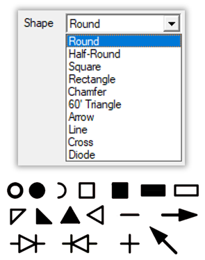 Layer: Selects the layer assignment for symbols. Some symbols, such as Diode and Arrow can only be added to silkscreen and assembly layers. 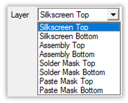 Outline Width: Silkscreen and assembly symbol line width should match the master line widths. Fill: When checked, creates a solid feature. Fill is not available for diodes or half circles. Size: This option can be specified in one of three ways: Diameter, for round features; Height and Width, for square and rectangular features; Size for Line, Cross, Chamfer, 60' Triangle and Diode; Base (the arrow base) for Arrow. Orientation: This option may be specified, with limitations, to some shape types. Placement X and Y: The X and Y numeric controls may be used to locate or relocate the symbol. Clicking on one of the "target" icons resets the value to zero. The F2 key may be used to capture an X-Y location prior opening the Symbol menu. 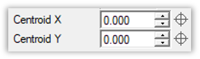 Keep-out Creation 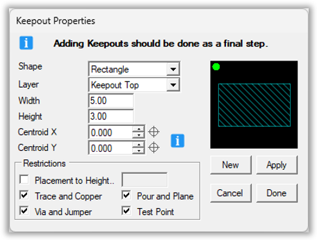 Shape: Basic Keep out available shapes are round, square and rectangular. 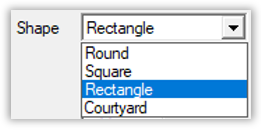 A notable exception is the Courtyard option. This option creates a keep out that mirrors the courtyard allowing restrictions that can be applied to the entire footprint. 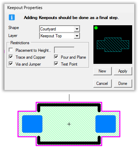 Layer: Selects the layer assignment for keep outs. 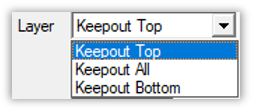 Placement X and Y: The X and Y numeric controls may be used to locate or relocate the keep-out. Clicking on one of the "target" icons resets the value to zero. The F2 key may be used to capture an X-Y location prior opening the Keep-out menu. 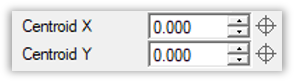 Restrictions: Defines the feature types that will not be allowed within the keep-out area. Placement Height is the maximum allowable height of any object within keep-out area. 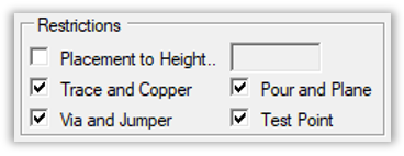 Symbol and Keep-out Properties Apply: This button will add a highlighted current symbol or keep-out feature to the footprint. When highlighted, the feature will continue to be subject to changes made and can be updated any time buy click apply. New: This button will instantiate an applied feature and initiate a feature of the same type (symbol or keep-out). This makes it unnecessary to close and reopen a menu in order to define and add a new feature. Cancel: This button will abort any feature currently in progress and return to the start menu configuration. Done: Closes the feature's menu. Upon closing, a reminder message will be displayed for features that have not been applied. General: Right-clicking on any symbol or keep-out feature will allow selection of a Properties dialog box, which just happens to be the Creation tool menu, allowing a full editing capability of the selected feature. 
 The Footprint Expert automates footprints to perfection. Professional, detailed, and accurate parts - all built consistently with identical rules, regardless of how many people are involved in your library development. Get your FREE Footprint Calculator or Footprint Expert Evaluation License: https://www.pcblibraries.com/Register" rel="nofollow - https://www.PCBLibraries.com/Register Call us - 847-557-2300 ------------- Stay connected - follow us! https://twitter.com/PCBLibraries" rel="nofollow - X - http://www.linkedin.com/company/pcb-libraries-inc-/" rel="nofollow - LinkedIn |