How To Choose the Footprint for SMD Chip Resistor
Printed From: PCB Libraries Forum
Category: PCB Footprint Expert
Forum Name: Questions & Answers
Forum Description: issues and technical support
URL: https://www.PCBLibraries.com/forum/forum_posts.asp?TID=3630
Printed Date: 28 Jun 2026 at 7:28pm
Topic: How To Choose the Footprint for SMD Chip Resistor
Posted By: Ariel_Levy
Subject: How To Choose the Footprint for SMD Chip Resistor
Date Posted: 22 Mar 2026 at 5:07am
|
How do you choose
the footprint for SMD Resistor case 0402? Vishay have
3 recommendations for footprints. Yageo one recommended but it’s different from Vishay. Vishay recommendation: L=0.50 A=0.40 B=0.60 BASED ON
IPC-7351 L=0.40 A=0.55 B=0.60 BASED ON IEC 61188-6-2 L=0.55 A=0.35 B=0.55 Yageo L=0.50 A=0.50 B=0.60 I am very confused by all the recommendations. I would appreciate a suggestion or any guidance on how to choose a footprint. |
Replies:
Posted By: Tom H
Date Posted: 22 Mar 2026 at 8:14am
|
IPC-7351 uses Min/Max Mode technology. the resulting footprint takes into consideration the package tolerances to calculate the pad stacks. The solder pattern should accommodate the package in the minimum, nominal and maximum material condition. The average 0402 tolerance range is +/-0.05 to +/-0.10. It seems like component manufacturers use their nominal package dimensions and add a Toe, Heel and Side. They use Nominal Mode technology and ignore the tolerances they provide in their datasheets. The average dimensions on an 0402 are L=1.00, W=0.50, T=0.25. Your pad stack pattern will depend on what dimensions and tolerances you use. However, if you run into a 0402 chip manufacturer that has tolerances greater than 0.10, I would highly question the accuracy of their machine process. Ideally, manufacturers try to produce packages that are Nominal Material Condition. That's the goal. Maybe in the future package tolerances will be 0.00 and then the Nominal Mode technology will take over and the IPC-7351 mathematical model will be history. ------------- Stay connected - follow us! https://twitter.com/PCBLibraries" rel="nofollow - X - http://www.linkedin.com/company/pcb-libraries-inc-/" rel="nofollow - LinkedIn |
Posted By: feynman
Date Posted: 22 Mar 2026 at 10:14am
| Ask a/your assembler. They probably assembled millions of parts and are probably the best source for a reliable footprint. |
Posted By: Ariel_Levy
Date Posted: 23 Mar 2026 at 12:58am
Tom thank you very much  and thank you Feynman
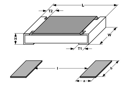
My difficulty is in obtaining information the thickness of the contacts size of the component (the size "T") I bought the IPC-7351 and 7352. and you don't have information about this. I think to buy EIA-JEP95 , and don't know it's worth the money if very MFG design is contacts size what "he" want's. This table i found is accurate? 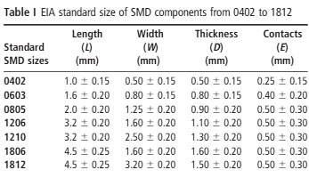 How you handle this with general discrete components ,when the contacts size can be between 0.10 to 0.40? With the IPC-7351 when contacts size is 0.4 mm?
|
Posted By: Tom H
Date Posted: 23 Mar 2026 at 8:46am
|
Here is the original EIA PDP-100 Chip Package dimensions and tolerances. https://www.pcblibraries.com/Forum/chips_topic3598.html%20" rel="nofollow - https://www.pcblibraries.com/Forum/chips_topic3598.html Compare with IEC. ------------- Stay connected - follow us! https://twitter.com/PCBLibraries" rel="nofollow - X - http://www.linkedin.com/company/pcb-libraries-inc-/" rel="nofollow - LinkedIn |