Chips
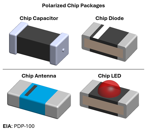
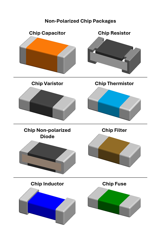
Chips: An ultra-compact rectangular housing designed specifically for surface mount discrete passive or semiconductor devices containing exactly two electrical terminals. Electrical contacts are located at opposite ends of the body, wrapping around the edges to form metallized soldering pads. Most 2-pin passive chips are physically symmetrical, allowing automated pick-and-place systems to orient them easily without top-to-bottom or front-to-back errors. The body typically consists of a single block of ceramic (for capacitors), thick-film substrate (for resistors), or molded plastic/glass (for diodes).
Monolithic Structure: The body typically consists of a single block of ceramic (for capacitors), thick-film substrate (for resistors), or molded plastic/glass (for diodes).
Rectangular or Square End-Cap Terminations: Electrical contacts are located at opposite ends of the body, wrapping around the edges to form metallized soldering pads.
Symmetrical Design: Most 2-pin passive chips are physically symmetrical, allowing automated pick-and-place systems to orient them easily without top-to-bottom or front-to-back errors.
|
Chip Size Codes
with Inch Dimensions
|
|
EIA Inch
(IEC Metric)
|
Inch Dimensions
|
|
01005 (0402)
|
0.0157 in × 0.0079 in
|
|
0201 (0603)
|
0.024 in × 0.012 in
|
|
0402 (1005)
|
0.039 in × 0.020 in
|
|
0603 (1608)
|
0.063 in × 0.031 in
|
|
0805 (2012)
|
0.079 in × 0.049 in
|
|
1008 (2520)
|
0.098 in × 0.079 in
|
|
1206 (3216)
|
0.126 in × 0.063 in
|
|
1210 (3225)
|
0.126 in × 0.098 in
|
|
1806 (4516)
|
0.177 in × 0.063 in
|
|
1812 (4532)
|
0.180 in × 0.130 in
|
|
2010 (5025)
|
0.197 in × 0.098 in
|
|
2512 (6332)
|
0.250 in × 0.130 in
|
|
2920 (7451)
|
0.290 in × 0.200 in
|
|
Chip Size Codes
with Metric Dimensions
|
|
IEC Metric (EIA
Inch)
|
Metric
Dimensions
|
|
0402 (01005)
|
0.40 mm × 0.20 mm
|
|
0603 (0201)
|
0.60 mm × 0.30 mm
|
|
1005 (0402)
|
1.00 mm × 0.50 mm
|
|
1608 (0603)
|
1.60 mm × 0.80 mm
|
|
2012 (0805)
|
2.00 mm × 1.25 mm
|
|
2520 (1008)
|
2.50 mm × 2.00 mm
|
|
3216 (1206)
|
3.20 mm × 1.60 mm
|
|
3225 (1210)
|
3.20 mm × 2.50 mm
|
|
4516 (1806)
|
4.50 mm × 1.60 mm
|
|
4532 (1812)
|
4.50 mm × 3.20 mm
|
|
5025 (2010)
|
5.00 mm × 2.50 mm
|
|
6332 (2512)
|
6.40 mm × 3.20 mm
|
|
7451 (2920)
|
7.40 mm × 5.10 mm
|
Performance & Manufacturing Challenges
Tombstoning Risk: Because these chips have only two terminals, an imbalance in surface tension during solder reflow can cause the component to lift off one pad and stand vertically like a tombstone. This is minimized by maintaining perfectly symmetrical landing pads and thermal reliefs.
Ultra-Low Parasitics: The absence of long lead wires reduces parasitic inductance and capacitance, making these packages ideal for high-speed signal integrity and high-frequency RF layouts.
High-Speed Placement: Their flat, symmetrical shapes make them highly optimized for automated vacuum pick-and-place nozzles, allowing assembly machines to shoot thousands of these components per minute.
Molded Body
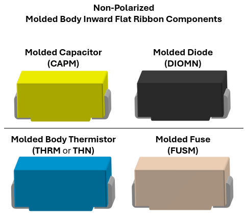
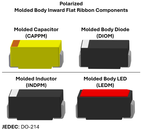
Molded Body: Electronic component housings formed by encapsulating internal elements (such as a silicon die, a capacitor element, or a lead frame) in a solid, injection-molded thermoset plastic or epoxy resin. Unlike generic ceramic or open-frame structures, these packages provide an airtight, structurally rigid shield that safeguards components against moisture, physical impact, and operational vibration.
Inward L-Bend Lead: The leads curl tightly underneath the molded plastic shell. This saves valuable PCB area, though it hides the solder joints from easy optical inspection.
Heel and Toe Goals: IPC guidelines dictate robust calculation values for the Toe (outer edge) and Heel (inner edge) of the pad. These parameters ensure that the solder fillet achieves high mechanical joint strength.
Side Goal Omission: For many molded body components – specifically those utilizing Inward L-Bends – IPC standards omit a side-joint goal requirement. Adding extra pad width along the sides does not increase mechanical hold. Furthermore, excess side solder can cause the component to float or rotate out of alignment during the reflow oven cycle.
|
Common
Molded Body Tantalum Capacitors
|
|
EIA
Size Code
|
Package
Dimensions
|
KEMET
Code
|
AVX
Code
|
|
2012-12
|
2.00 x 1.30 x 1.20
|
R
|
R
|
|
3216-10
|
3.20 x 1.60 x 1.00
|
I
|
K
|
|
3216-12
|
3.20 x 1.60 x 1.20
|
S
|
S
|
|
3216-18
|
3.20 x 1.60 x 1.80
|
A
|
A
|
|
3528-12
|
3.50 x 2.80 x 1.20
|
T
|
T
|
|
3528-21
|
3.50 x 2.80 x 2.10
|
B
|
B
|
|
6032-15
|
6.00 x 3.20 x 1.50
|
U
|
W
|
|
6032-28
|
6.00 x 3.20 x 2.80
|
C
|
C
|
|
7260-38
|
7.30 x 6.00 x 3.80
|
E
|
V
|
|
7343-20
|
7.30 x 4.30 x 2.00
|
V
|
Y
|
|
7343-31
|
7.30 x 4.30 x 3.10
|
D
|
D
|
|
7343-43
|
7.30 x 4.30 x 4.30
|
X
|
E
|
Key Physical Features - Fully Encapsulated Core: Thermoset epoxy compound forms a solid protective layer on all sides, completely insulating the sensitive inner structures (such as silicon dies, wound wires, or sintered tantalum pellets) from environmental elements.
- Integrated Polarity Markers: Because the body is formed in an injection-molding process, bevels, chamfered corner notches, or deep laser-etched bands are built directly into the plastic to indicate polarity (essential for diodes and tantalum caps).
- Wrap-Around or Inward Terminations: Leads typically exit the bottom or centerline of the plastic molding and are bent flat against the body ends or tucked flush as leadless bottom contacts.
- Classifications & Examples: Molded body packages use unique design rules and prefixes to accurately map their footprint requirements.
Tantalum Capacitors (CAPMP / EIA Standard): Features highly standardized molded packages categorized by standard uppercase lettering. - A Case (3216 Metric): 3.20 mm x 1.60 mm nominal
- B Case (3528 Metric): 3.50 mm x 2.80 mm nominal
- C Case (6032 Metric): 6.00 mm x 3.20 mm nominal
- D Case (7343 Metric): 7.30 mm x 4.30 mm nominal
Diodes (DIOM / JEDEC DO-214): Molded discrete diodes leverage robust, wide wrap-around terminal feet built to absorb thermal stress. - SMA (DO-214AC): Smallest common molded diode variant
- SMB (DO-214AA): Medium profile option
- SMC (DO-214AB): Largest footprint format supporting high power surge ratings
Engineering Design Parameters: When laying out a land pattern for a molded body part with Footprint Expert use distinct math models. - Molded Body Side Goal: Footprint generation tools use a unique variable known as the "Molded Body Side Goal" to ensure the copper landing pads extend far enough beyond the side boundaries of the plastic block, keeping the solder joint from bridging or starving.
- Heel Fillet Compensation (Jh): Because molded leads often tuck close or underneath the plastic shell, the heel fillet calculations must account for package chamfering to prevent cold solder joints or component tilt.
- Robust Placement Courtyard: Since the molding process can incur minor edge tolerances (+/-0.2 mm package deviations), the IPC placement courtyard boundary must be generous enough to account for physical variations during automated assembly pick-and-place tracking.
Performance Advantages - High Moisture Resistance: Direct plastic encapsulation eliminates internal air pockets, effectively blocking moisture ingress and saving parts from internal corrosion or short circuits.
- Structural Resistance to Shock: The solid core cushions internal components from physical drops, heavy vibrations, and handling damage during rapid assembly lines.
- Perfect Coplanarity Control: Flat molded bottoms provide a highly stable seating plane during reflow, significantly reducing defects like skewing or uneven floating.
- Cost Efficiency: Plastic transfer molding remains the most affordable, mass-producible chip encapsulation method in modern electronics manufacturing
Metal Electrode Leadless Face (MELF)
Metal Electrode Leadless Face (MELF): A specialized surface mount component package characterized by a cylindrical body with metallized round end caps. Unlike standard rectangular chip components, MELF packages are round and do not use traditional leads. They are primarily used for high-reliability resistors, fuses and diodes where superior thermal stability, low noise, and excellent moisture resistance are required.
Cylindrical Body: The housing is a glass or ceramic tube, making it highly resistant to thermal shock and moisture
Leadless Endcaps: Metal caps wrap around the circular edges on both ends, serving as the soldering terminals.
No Orientation Issues: Because it is perfectly round, the component can rotate along its long axis during placement without affecting its electrical connection.
Superior Reliability: MELF components offer exceptionally low failure rates and excellent long-term stability under harsh conditions.
High Thermal & Power Handling: The cylindrical shape provides a larger surface area than flat chips, allowing better heat dissipation and higher power ratings.
Low Noise & Parasitic: Excellent for high-frequency or high-precision circuits due to minimal structural inductance and capacitance.
|
Common MELF Package Sizes
|
|
Common Case Names
|
Size Code
|
Package Dimensions
|
|
MicroMelf
(MMU)
|
0102
|
2.20 L x 1.10 Dia.
|
|
MiniMelf
(MMA)
|
0204
|
3.60 L x 1.40 Dia.
|
|
Melf
(MMB)
|
0207
|
5.80 L x 2.20 Dia.
|
Small Outline Diode (SOD) with Gullwing Leads Small Outline Diode (SOD) with Gullwing Leads: A standard surface mount semiconductor package designed for discrete components like switching, Schottky, and Zener diodes. 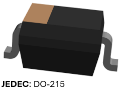 Lead Design Lead Design: The "Gullwing" description means the metal leads bent downward and then outward.
Soldering & Assembly: These leads provide solid footing on the copper pads during assembly. They are ideal for automated pick-and-place and reflow soldering but are also large enough to allow for relatively easy hand soldering.
Package Variants: This package style comes in various standardized sizes to accommodate different thermal requirements and spatial limitations.
Common Applications Include: Smartphones and wearable devices, IoT modules and compact consumer electronics, Power supply circuits and automotive modules, LED lighting drivers and signal conditioning.
|
Common Small Outline Diode (SOD)
Sizes
|
|
Case Code
|
Package Dimensions
|
|
SOD-123
|
3.68 mm x 1.17 mm x 1.60 mm
|
|
SOD-128
|
5.00 mm x 2.70 mm x 1.10 mm
|
|
SOD-323
|
1.70 mm x 1.25 mm x 0.95 mm
|
|
SOD-523
|
1.25 mm x 0.85 mm x 0.65 mm
|
|
SOD-723
|
1.40 mm x 0.60 mm x 0.59 mm
|
Small Outline Diode Flat Lead (SODFL) Small Outline Diode Flat Lead (SODFL): A compact, ultra-low-profile surface mount technology (SMT) semiconductor housing designed to replace standard Gullwing SOD packages. By utilizing flat, folded metal ribbons that lie completely flush beneath the bottom of the device rather than curve outward, it maximizes board space, increases power handling, and significantly lowers the component profile.
Core Advantages Over Gullwing Variants: - Space Saving: Eliminating extending Gullwing leads shrinks the necessary circuit board footprint. For example, an SOD-123FL serves as a direct drop-in replacement on existing pads but reduces physical component clearance.
- Superior Thermal Performance: Because the flat leads are positioned directly underneath the component body, the heat dissipation path to the PCB copper pads is incredibly short. This design offers up to 25% lower thermal resistance compared to standard packages.
- Ultra-Low Profile: These packages typically feature a maximum height profile of just 1.00 mm to 1.20 mm. This represents a profile reduction of 25% or more compared to traditional alternatives, making them ideal for high-density stack-ups.
- Increased Surge Capacity: Many flat lead designs incorporate an internal clip-attach structure rather than fragile wire bonds. This structural change boosts transient forward surge-current survival.
Common Applications: The combination of enhanced thermal dissipation and minimized Z-axis height makes SODFL variants highly desirable for: - Portable Electronics: Ultra-thin smartphones, smartwatches, and portable power banks.
- Power Conversion: Secondary rectification and freewheeling diodes in compact AC/DC or DC/DC converters.
- Circuit Protection: High-efficiency Schottky rectifiers, Zener voltage stabilizers, and Transient Voltage Suppression (TVS) applications.
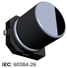
Capacitor, Aluminum Electrolytic (CAPAE) Capacitor, Aluminum Electrolytic (CAPAE): A specialized housing used for components that provide high volumetric capacitance in a relatively compact space. Constructed by winding an anode foil, paper separators saturated with liquid electrolyte, and a cathode foil into a cylinder, these packages are polarized and feature distinct physical markers to indicate the negative terminal.
Unlike monolithic ceramic capacitors, these parts are housed in distinct mechanical form factors dictated by their mounting style, ripple current capability, and spatial constraints.
SMD aluminum electrolytic capacitors are typically packaged in cylindrical metallic aluminum "cans" sitting atop a square, black plastic insulating base. The base bends the terminal leads flat under the component body to create solder pads for reflow soldering.
Polarity Indicator: A highly visible black or dark colored crescent/stripe painted directly onto the top face of the metallic cylinder denotes the negative pad.
|
Common
Aluminum Electrolytic Capacitor Sizes
|
|
Case Code
|
Diameter
x Height
|
Common
Values
|
|
A
|
4.00 mm x 5.40 mm
|
1uF to 10uF (50V)
|
|
B
|
5.00 mm x 5.40 mm
|
10uF to 22uF (35V)
|
|
C
|
6.30 mm x 5.40 mm
|
47uF to 100uF (16V)
|
|
D
|
6.30 mm x 7.70 mm
|
100uF to 22uF (25V)
|
|
F
|
8.00 mm x 10.20 mm
|
220uF to 470uF (35V)
|
|
G
|
10.0 mm x 10.20 mm
|
470uF to 1000uF (16V)
|
Crystals (XTAL)
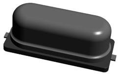
Crystals (XTAL): A specialized, surface mount housing designed for passive timing components. Unlike multi-pin active oscillators that require separate power, a 2-pin crystal package only contains the raw quartz blank and two electrical terminals. It relies entirely on the microcontroller's internal inverter circuit to generate a clock signal.
Construction and Hermetic Sealing: Because quartz crystals are highly sensitive to moisture, dust, and atmospheric pressure changes, the packages utilize a hermetic (airtight) seal. - The Body: The base is typically constructed from a multi-layer technical ceramic material.
- The Lid: A metal seam-welded lid or a glass-sealed ceramic lid covers the top. This metal lid is often grounded internally or externally to shield the sensitive crystal blank from Electromagnetic Interference.
SMD crystal packages are standardized by their physical length and width dimensions. The industry has shifted heavily toward smaller footprints to fit dense modern electronics.
|
Common SMD Crystal Packages
|
|
Case Code
|
Package Dimensions
L x W x H Range
|
Typical Uses
|
|
5032
|
5.0 x 3.2 x 1.0 -1.20 mm
|
Microcontrollers
|
|
3225
|
3.2 x 2.5 x 0.7 - 0.90 mm
|
Ease
of Routing
|
|
2520
|
2.5 x 2.0 x 0.5 - 0.60 mm
|
loT Modules
|
|
2016
|
2.0 x 1.6 x 0.45 mm
|
Smartphones
|
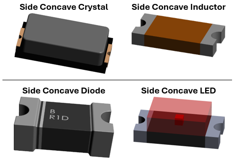
Side Concave Packages 2-pin Side Concave Packages: A surface mount electronic component housing where the electrical terminations or leads are recessed into indented, semicircular, or "scalloped" channels along the vertical sidewalls of the component body. Unlike standard convex component packages where leads protrude outward (like Gullwing leads) or flat surfaces, the concave architecture places the solderable terminals inside these inner grooves.
Assembly and Manufacturing Impact
- Solder Joint Integrity: Early designs favored concave configurations under the assumption that isolating the paste within the inner channel would mitigate solder bridging. Modern automated optical inspection (AOI) data shows that the absolute spacing on the PCB pad layout dictates bridging protection far more than the concave shape itself.
- No-Lead Visual Inspection: Certain modern variations of side concave packages overlap with side-wettable flanks seen in Dual Flat No-Lead (DFN) configurations. This recess allows solder paste to travel upward into the side groove, creating a visible fillet that validates a solid mechanical bond during high-speed assembly inspection.
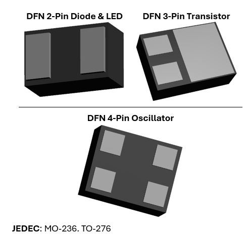
Dual Flat No-Lead (DFN) Dual Flat No-Lead (DFN): A surface mount electronic component housing with a near-zero profile that replaces traditional extending leads with flat, metal contact pads on its underside.
Key Design and Structural Features - Bottom-Surface Pads: Electrical contacts sit flush with the bottom plastic mold compound, eliminating vulnerable, bendable pins.
- Thermal Pad: Most DFN packages feature an exposed center metal pad that is soldered directly to the PCB to channel heat away from the silicon die.
- Ultra-Low Profile: The compact design minimizes component height and weight, making it ideal for mobile devices and high-density boards.
Performance Advantages - Excellent Thermal Dissipation: The exposed center pad creates a direct thermal highway, allowing high power processing in a tiny footprint.
- Low Parasitic Impedance: Eliminating long lead wires reduces internal resistance and inductance, enhancing high-frequency signal performance.
- Cost-Efficient: The simplified lead frame design uses less raw material and is highly cost-effective to manufacture at scale.
Assembly and Inspection Challenges - Hidden Solder Joints: Because the connections sit underneath the package, traditional visual inspection cannot verify electrical connectivity or find voids.
- Side-Wettable Flanks (SWF): Modern DFN variants feature a specialized cut or plating on the side edge of the pad. This allows solder to wick up the outer wall, creating a visible fillet for Automated Optical Inspection (AOI).
- Solder Mask and Stencil Design: Precise stencil opening design is required for the thermal pad to prevent "floating," where excess solder lifts the component and prevents the perimeter signal pads from making contact.
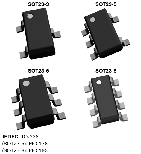
Small Outline Transistor SOT23 (SOT Form Factor) Small Outline Transistor SOT23 (SOT Form Factor): A highly popular, compact, plastic-molded surface mount device (SMD) package. Widely used for diodes, BJT transistors, MOSFETs, and voltage regulators, it features Gullwing leads extending from its two long sides and is favored for its space efficiency in modern electronics. Typically, 3 pins, though 5-pin (SOT23-5) and 6-pin (SOT23-6) variants are heavily used for small logic ICs and operational amplifiers. Because SOT-23 packages lack a dedicated thermal pad underneath, heat must be dissipated through the copper traces on the PCB. To optimize cooling, expand the copper connected to the pins (particularly the wider drain or collector pin).
|
Gullwing SOT23
Type Form Factor Component Families
|
|
EIA
|
JEITA
|
Pin Pitch
|
Pin Qty
|
|
SOT23-3
|
SC59
|
0.95
|
3
|
|
SOT28
|
SC70-8
|
0.65
|
8
|
|
SOT323
|
SC70
|
0.65
|
3
|
|
SOT346
|
SC59A
|
0.95
|
3
|
|
SOT353
|
SC88A
|
0.65
|
5
|
|
SOT363
|
SC88
|
0.65
|
6
|
|
SOT416
|
SC75
|
0.50
|
3
|
|
SOT753
|
SC74A
|
0.95
|
5
|
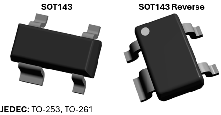
Small Outline Transistor SOT143 (SOT) Small Outline Transistor SOT143 (SOT): A low-profile, plastic surface mount package featuring four Gullwing leads. Derived directly from the standard SOT-23 geometry, it is uniquely characterized by having one lead that is visibly wider than the other three. This asymmetrical pin layout enforces a built-in reverse-polarity protection, making it a staple for high-frequency radio frequency (RF) transistors, Schottky/PIN diodes, TVS protection arrays, and voltage supervisor circuits.
PCB Design & Footprint Guidelines - Orientation Verification: Because of the asymmetrical fourth lead, CAD footprint library creation must map exactly to the manufacturer's pinout. The wider pad acts as an un-cloneable indicator for automatic vision-inspection and pick-and-place indexing.
- RF Grounding & Thermal Benefits: The broadened lead is not just a layout guide; it dramatically drops package inductance. This provides an exceptionally clean ground path for RF designs. Furthermore, it serves as the package’s primary thermal conduit to the board, so pulling a substantial copper pour out from this wide pad is recommended.
- Solder Bridging Risk: Although the side-to-side pitch is spacious, the end-to-end clearance requires exact solder mask dam tracking to prevent solder bridging across the small gaps
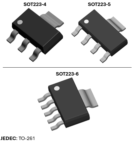
Small Outline Transistor SOT223 (SOT) Small Outline Transistor SOT223 (SOT): A medium-power, plastic surface mount device package. It is widely chosen for discrete semiconductors and integrated circuits that require robust thermal handling in a compact layout, such as linear voltage regulators, power MOSFETs, and load switches.
Key Physical Characteristics
- Lead Configuration: It typically features four leads total: three standard Gullwing pins on one side of the body and one large, exposed tab on the opposite side.
- The Thermal Tab: The large tab is mechanically and electrically continuous with the center pin (Pin 2). It provides a direct, low-resistance thermal path to conduct heat away from the silicon die into the PCB.
- Body Dimensions: The main plastic body measures roughly 6.50 mm x 3.50 mm with an overall profile height of 1.65 mm. Including the leads, the total width span is approximately 7.00 mm.
- Pin Pitch: The distance between the centers of the three adjacent pins is 2.30 mm for 4-pin and 1.50 mm for 5-pin and 1.27 for 6-pin.
PCB Footprint & Layout Guidelines - Thermal Management & Copper Pour: Because the package dissipates more power than smaller standard packages like the SOT-23, its performance relies heavily on your PCB layout.
- Connect a large copper pour directly to the pad of the large thermal tab.
- Drop a matrix of thermal vias into the tab pad to transfer heat to internal or bottom-side ground/power planes. Without adequate copper area, the component will overheat and trigger thermal throttling or fail prematurely.
- Electrical Isolation Considerations: The large tab is typically tied to a specific net (often Vout or GND), depending on the component). Ensure that neighboring signal traces or component pads maintain safe electrical clearance from the enlarged copper pour surrounding this tab pad.
- Soldering and Solder Mask: Because the pin pitch is a relatively wide 2.30 mm, the package is highly forgiving for both automated assembly line reflow ovens and manual prototyping hand-soldering. However, ensure your footprint includes a precise solder mask cutout for the thermal tab to prevent solder pooling from shifting the smaller pins out of alignment during reflow.
Small Outline Flat Lead (SOFL) Small Outline Flat Lead (SOFL): A surface mount integrated circuit (IC) package characterized by a low-profile rectangular body and flat, non-extended leads rather than standard protruding Gullwing pins. It bridges the gap between traditional small outline packages (SOP/SOIC) and bottom-termination flat packs, providing a space-efficient layout tailored for tight vertical clearances and high-frequency, automated PCB assembly. 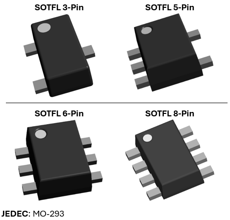 Key Physical Features Key Physical Features- Flat Lead Structure: The leads do not wrap or form distinct Gullwings. They lie flush against the underside or periphery of the device, which minimizes parasite inductance.
- Dual-Sided Orientation: Pins or landing pads typically extend along two opposite sides of the rectangular body.
- Low Profile: The "Flat" designation prioritizes a thin z-axis height, perfect for tight enclosures like laptops, memory modules, and portable smart devices.
- Exposed Thermal Pad (Often Included): Many variations incorporate an internal die attach paddle exposed on the bottom side. This pad solders directly to the PCB to conduct heat away efficiently.
Design Parameters When creating an IPC-7351 standardized land pattern for an SOFL package, engineers focus on several specific features: - Pitch: Typically ranges between 0.50 mm to 1.00 mm depending on the subcategory variant.
- Pads: Footprints require flat, rectangular SMD copper pads.
- Solder Mask: Non-Solder Mask Defined (NSMD) pads are preferred to guarantee high registration accuracy.
Performance Advantage - High Signal Integrity: Shorter, flatter leads drastically lower parasitic capacitance and inductance, making them superior for high-speed switching applications.
- Excellent Heat Dissipation: Direct bottom-pad soldering turns the PCB's ground planes into large heat sinks via thermal vias.
- Space Efficiency: Frees up vertical height and tighter pitch allows dense layout clustering.
DPAK DPAK: A standard surface mount transistor package designed for high-power semiconductor devices. It features a large metal tab that solders directly to the PCB to dissipate heat. It is widely used for voltage regulators, MOSFETs, and power diodes. 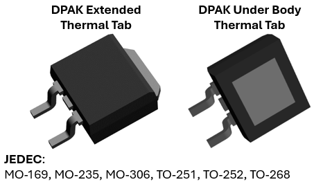 Key Physical Features Key Physical Features- Thermal Tab: A large metal backside tab acting as the primary drain/collector connection and heat sink.
- Three-Terminal Layout: Typically features two smaller leads and one large clipped lead or tab.
- Surface Mount Design: Eliminates the need for through-holes, speeding up automated assembly.
Design Parameters - Lead Pitch: Standard distance between the smaller pins is 2.30 mm (0.090 inches).
- Thermal Vias: Footprints require an array of vias under the tab to transfer heat to internal copper layers.
- Solder Paste Stencil: The large tab pad requires a windowpane stencil pattern to prevent component floating and solder splattering.
Performance Advantages - High Power Handling: Safely manages higher currents and voltages than standard small-outline packages.
- Low Thermal Resistance: Direct copper-to-copper bonding ensures rapid heat transfer away from the silicon die.
- Robust Mechanics: The large soldered surface area provides high mechanical stability against vibration.
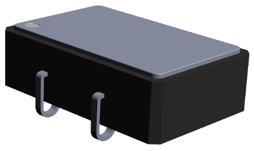
Oscillator, J-Lead (OSCJ) Oscillator, J-Lead (OSCJ): A surface mount, plastic-molded enclosure specifically designed for crystal oscillators, clock generators, and frequency control devices. It adapts the traditional Small Outline J-Lead (SOJ) format into a 4-pin or 6-pin specialized housing, featuring pins that curl downward and inward beneath the device body resembling the letter "J". This configuration provides an alternative to standard leadless ceramic packages (LCC) by adding robust mechanical flexing capabilities to critical timing circuits.
Key Physical Features - Inward-Curled J-Leads: Unlike protruding Gullwing leads that extend outward, J-leads tuck directly under the plastic body. This structural choice saves significant board real estate over standard SOIC components.
- Plastic Molded Body: Typically features a rugged, molded plastic encapsulation housing the quartz crystal blank and its active oscillation IC circuitry.
- Standardized Pinouts: Usually configured as a 4-pin or 6-pin module. In a standard 4-pin configuration, the pinouts follow this layout:
- Pin 1: Tri-State Enable/Disable or No Connect
- Pin 2: Ground (GND)
- Pin 3: Output Frequency Clock
- Pin 4: Supply Voltage (VDD)
Design Parameters When laying out a land pattern for an OSCJ component on a board, designers prioritize the following IPC-compliant geometries: - Footprint Pads: The copper pads must extend slightly outward and inward relative to the J-lead apex to guarantee a proper solder fillet formation along both the inner and outer curve of the lead.
- Pitch: Large-form plastic OSCJ packages typically leverage a generous lead pitch, commonly at 2.54 mm or 5.08 mm, ensuring high electrical isolation between high-frequency outputs and supply traces.
- Common Dimensions: These packages are usually larger than modern ceramic variants, with a popular historical standard footprint measuring roughly 14.00 mm x 9.8 mm.
Performance Advantages - Thermal & Shock Compliance: The J-lead structure functions like a miniature spring. This flexibility absorbs mechanical shock, vibration, and Coefficient of Thermal Expansion (CTE) mismatches better than rigid, leadless ceramic packaging.
- Solder Joint Visual Inspection: Because the J-lead curls along the outer side of the body, the solder heel and toe fillets remain visibly accessible for automated optical inspection (AOI).
- High Pre-Solder Resiliency: The tucked lead geometry keeps the component leads protected from accidental bending or misalignment during shipping, tape-and-reel feeding, or handling prior to reflow.
Oscillator, L-Lead (OSCL) Oscillator, L-Lead (OSCL): A surface mount enclosure designed for quartz crystal oscillators and clock generators. It features L-shaped leads that extend outward and bend downward to form a flat seating plane flush with the PCB surface. This geometry mimics a standard Gullwing style but is specialized for the weight, height, and frequency constraints of surface mount timing modules. 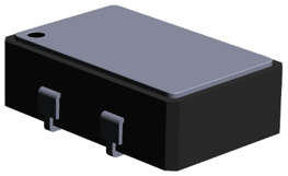 Key Physical Features Key Physical Features- Outward-Extended L-Leads: Leads protrude from the sides of the package and bend downward and outward, forming an "L" shape.
- Highly Visible Solder Fillets: The extended foot of the "L" lead sits entirely outside the component body outline, allowing for straightforward automated visual inspection.
- 4-Pin or 6-Pin Layout: Typically follows standard oscillator pin configurations (VDD), Ground, Output, and Enable/Disable).
Design Parameters - Footprint Pad Extension: Land patterns require a longer pad length extending beyond the lead tip (toe) to ensure a strong solder fillet.
- Pitch Standards: Typically features a standard pitch of 2.54 mm or 1.27 mm for robust isolation of high-frequency clock signals.
- Coplanarity: Requires strict lead coplanarity tolerance (usually within 0.10 mm) to ensure all L-feet sit perfectly flat on the solder paste during reflow.
Performance Advantages - Superior Solder Joint Inspection: Unlike leadless (LCC) or J-lead variants, the entire solder joint is fully visible from above, making it highly compatible with basic Automated Optical Inspection (AOI) systems.
- Excellent Mechanical Reworkability: The exposed outward leads make it one of the easiest oscillator packages to rework, manually desolder, or probe during debugging.
- Stress Relief: The bend in the L-lead provides mild compliance, absorbing physical board flex and thermal expansion stresses better than leadless ceramic packages.
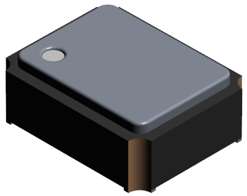
Oscillator, Corner Concave (OSCCC)
Oscillator, Corner Concave (OSCCC): A standardized, surface mount ceramic or plastic packaging format designed specifically for highly miniaturized crystal oscillators and clock generators. Rather than using extended metal leads like J-leads or Gullwing pins, an OSCCC package utilizes castellated solder pads recessed directly into the vertical corners of the component's body. This design maximizes component density on dense circuit boards while ensuring robust high-frequency electrical isolation. Key Physical Features - Corner Castellations (Concave Terminals): Solder contacts form semi-cylindrical metallized grooves or scallops on the outermost four corners of the device. Solder wicks up these inner vertical channels during reflow.
- Leadless Profile: The total absence of outward-extending leads eliminates risk of bent pins, ensuring a completely flat bottom seating plane.
- Hermetically Sealed Body: Usually constructed with a ceramic substrate capped by a metal lid to insulate the sensitive internal quartz resonator or MEMS core from atmospheric moisture and environmental aging.
- Standard 4-Pin Output: The classic corner configuration natively routes the standard 4-pin functional diagram:
- Corner 1: Tri-state Control / Enable / No Connect
- Corner 2: Ground (GND)
- Corner 3: Frequency Output Clock Signal
- Corner 4: Supply Voltage (Vpp)
- Pad Geometry: PCB landing pads are placed directly underneath each corner. They must extend slightly outward beyond the component perimeter to accommodate the side solder fillet.
- Silkscreen Expansion: Because the metal pads occupy the actual corners of the rectangular body, layout engineers must provide an expanded or modified silkscreen outline to ensure the component outline remains visible during manual inspection.
- Pin 1 Indicator: Due to tightly packed corner spaces, standard circular silkscreen dots may conflict with the copper pads; specialized footprint rules apply to shift the Pin 1 indicator clear of the solder joints.
Performance Advantages - Ultra-Low Parasitic Inductance: The direct corner contact pathway eliminates the inductive loop area inherent to long J-leads or L-leads, preserving signal integrity for high-speed GHz-range clock signals.
- Excellent Solder Fillet Inspection: Because the metallized contact curves up the vertical outer corner edge, inspection cameras can verify a robust, shiny solder joint heel from the side via Automated Optical Inspection (AOI).
- Maximum Density Space Savings: Features one of the smallest package envelopes available for clock circuits, saving substantial PCB space compared to plastic-molded leaded components.
- Self-Alignment: Surface tension from the molten solder paste pulls the corner cutouts uniformly onto the target footprints during reflow oven cycles, minimizing skewing or rotational placement errors.
Oscillator, Side Concave (OSCSC) Oscillator, Side Concave (OSCSC): A standardized, surface mount ceramic or plastic packaging format for quartz crystal oscillators and clock generators. It features castellated solder pads recessed into the flat side edges of the component's body rather than the corners. This design offers a compact, leadless layout that optimizes trace routing and signal path isolation. 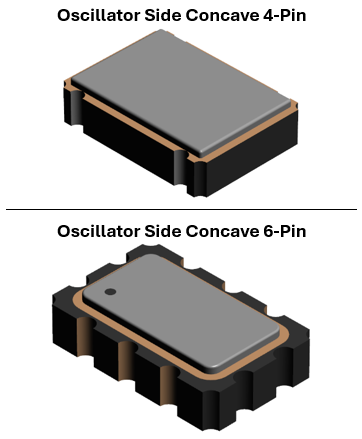 Key Physical Features Key Physical Features- Side Castellations (Concave Terminals): Semi-cylindrical, metallized grooves are located along the long or short side edges of the rectangular housing. Solder wicks up these inner vertical channels during reflow.
- Leadless Profile: The absence of protruding metal pins eliminates the risk of bent leads, providing a completely flat underside seating plane.
- Hermetically Sealed Substrate: Constructed with a rugged ceramic body and a metal lid to protect the internal quartz or MEMS resonator from mechanical stress and moisture.
IPC Footprint & Design Parameters According to IPC-7351B package standards, the naming format follows OSCSC + Length × Width × Height – Pin Count: - Pad Geometry: PCB land pads are positioned flush with the side walls of the oscillator. Pads must extend outward slightly past the package edge to allow a visible side solder fillet to form.
- Signal Isolation: Placing pads on the sides keeps the component corners clear, allowing routing traces or ground shield fills to pass cleanly around the corners of the component body.
- Pin 1 Orientation: Because the pads sit mid-side, the package corners are ideal for clear silkscreen dots or chamfered edges to mark Pin 1.
Performance Advantages - Minimized Parasitic Inductance: Short, leadless contact paths minimize inductive loops, ensuring stable performance for high-frequency clock signals.
- Side-Fillet Optical Inspection: Solder wicks into the side concave channels, allowing easy verification of a robust joint via Automated Optical Inspection (AOI).
- Self-Alignment: Surface tension from molten solder draws the side castellations symmetrically onto the PCB land pads, reducing component rotation or shifting during reflow.
- Board Space Efficiency: Offers a very tight, low-profile footprint ideal for dense hardware layouts like telecommunication modules, networking cards, and single-board computers.
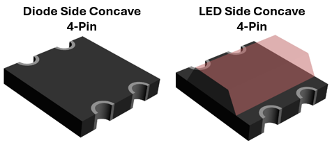
Side Concave (4-Pin) Diode and LED Side Concave (4-Pin) Diode and LED: A specialized, leadless surface mount footprint standard defined by IPC-7351. Instead of utilizing standard peripheral leads or bottom pads, this package features four metallized semi-cylindrical cutouts (castellated grooves) recessed symmetrically into the side walls of its ceramic or epoxy body. It is primarily implemented for multi-diode arrays and multi-color RGB LEDs, where vertical board profile, trace isolation, and optical inspection are paramount.
Key Physical Features
- Side-Wall Castellations: The electrical contacts curve upward along the vertical perimeter, creating a concave indentation on the left and right sides.
- Low-Profile Leadless Structure: Eliminating outward-facing pins lowers the package clearance, saving surface space and preventing accidental lead bending or damage during automatic component picking.
- Polarized Geometries: Components utilize an uneven chamfered corner, a molded notch, or an offset keyway pin configuration to denote diode cathode placement and prevent reverse assembly orientation.
Common Electrical Configurations Because this package format breakout provides four distinct terminal points, it typically services two component families: - Multi-Color (RGB) LEDs: Houses a shared internal node alongside separate color dies. Semicustom variants break out as either a Common Anode configuration (one positive terminal, three separate color cathodes) or a Common Cathode configuration.
- Integrated Diode Bridges / Arrays: Integrates a series of four independent rectifier diodes or protection Zeners mapped in a single network (e.g., standard full-wave bridge rectifier or multi-channel ESD clamping array).
Footprint & PCB Layout Parameters When defining this component footprint inside CAD suites like Altium Designer or IPC Footprint Expert, engineering rules mandate precise layout specs: - Pad Extension (Toe Out): PCB land copper must extend beyond the physical side walls of the device housing. This ensures molten solder paste wicks upward into the semicircular channel, generating a visible heel fillet.
- Solder Mask Openings: Footprints require Non-Solder Mask Defined (NSMD) clearances around the side terminals to prevent masking material from encroaching into the castellated pocket, which could cause cold-joint connectivity failure.
- Clearance Routing: By keeping the outer corners of the rectangular component body free of metallic terminals, designers can safely route signal traces or drop ground via anchors right up against the corners of the housing envelope without risk of short-circuiting.
Performance Advantages - Robust Optical Inspection (AOI): Automated optical cameras can easily view the solder fillet ascending the vertical side channel from a top-down or slight-angle camera perspective, an option missing from under-body LGA packages.
- Self-Centering Properties: During the reflow oven process, liquid surface tension pulling on all four concave pockets naturally realigns the chip center directly onto the target pads, reducing rotational skewing or floating.
- Low Parasitic Loop Inductance: Shorter internal lead pathways significantly minimize high-frequency parasitics, allowing protection diodes to react to high-speed transients rapidly.
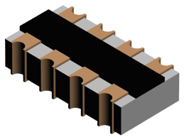
Side Concave Chip Array Side Concave Chip Array: A surface mount passive component housing that integrates a matrix of multiple discrete components – such as resistors or capacitors – into a single leadless chip. Rather than using protruding pins or flat bottom pads, it features multiple semi-cylindrical metallized grooves (castellations) recessed into its side walls. This format effectively places multiple independent components side-by-side in a single structural body to maximize assembly density and efficiency. Key Physical Features - Serrated Side Castellations: The left and right perimeter edges look like scallops or waves. The electrical terminations run up these vertical indentations, creating separate isolated contact pathways.
- Monolithic Rectangular Body: Constructed from a single piece of high-grade ceramic (co-fired alumina) or glass-epoxy material. This body isolates the internal passive elements from one another.
- Even Pin Distributions: Most commonly deployed in 4-pin (2-element), 8-pin (4-element), or 16-pin (8-element) configurations, with the contacts split symmetrically on opposite long sides.
Footprint & Naming Parameters These packages follow a precise naming structure to describe their physical boundaries, using the format RESCAV + Pin Count + P + Pitch _ Length x Width x Height + L Lead Width x Lead Length. Example: RESCAV8P127_500X200X70L40X80 - Pitch-Driven Layout: The spacing between the centers of adjacent side concave pads is tightly controlled, typically standardizing at 0.50 mm or 0.80 mm.
- Toe Pad Extension: PCB landing pads must extend outward beyond the physical perimeter of the ceramic body to ensure the solder forms a strong, rising vertical joint.
- Solder Mask Dams: Pocket clearances must have precise mask dams between the closely packed side-by-side pads to prevent solder bridging during reflow.
Performance & Manufacturing Advantages - High Packing Density: Combines up to eight individual resistors or capacitors into a single physical component footprint, saving significant board space over discrete layout methods.
- Excellent Solder Fillet Visibility: Solder naturally wicks up the side-wall concavities. This creates clear, visible fillets that are easily verified by Automated Optical Inspection (AOI) systems.
- Anti-Tombstoning: Small individual 0201 or 0402 discrete passives frequently stand up on one end during reflow (tombstoning) due to unbalanced solder forces. The larger, heavier monolithic body of a chip array completely eliminates this assembly defect.
- Trace Routing Paths: Because the terminations are confined strictly to the sides, the space underneath the array and around its outer corners remains completely clear, providing valuable routing room for underlying circuit traces.
|




 Post Options
 Thanks(0)
 Quote
Quote  Topic: Surface Mount Component Families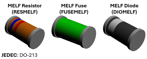




 Topic Options