

|
|
Wirebound inductor |
Post Reply 
|
| Author | |
dramos 
Advanced User 
Joined: 18 Feb 2021 Status: Offline Points: 81 |
 Post Options Post Options
") Thanks(0) Thanks(0)
 Quote Reply Quote Reply
 Topic: Wirebound inductor Topic: Wirebound inductorPosted: 03 Mar 2021 at 5:55am |
|
Hi to all:
I am trying to create a footprint of a wirebound inductor, Murata LQW18AN5N6G80D. I configured my component as an SMD/Chip/Inductor and as the metalization of the pin part is not the height of the component, I configured the height of the part as the height of the metalization. 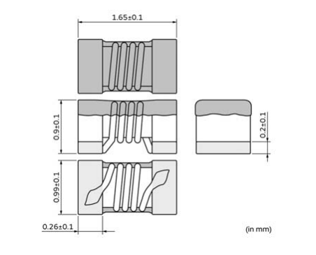 How do you resolve that kind of components? Thanks for your comments. dramos |
|
 |
|

|
|
|
|
|
Tom H
Admin Group 

Joined: 05 Jan 2012 Location: San Diego, CA Status: Offline Points: 5954 |
Post Options
Thanks(0)
Quote Reply
Posted: 03 Mar 2021 at 9:53am |
|
These Inductors are becoming more popular these days. There should be a mfr. recommended pattern for the footprint. If not, the pad size is:
Heel = 0.00 but you need to compensate for the +/- body length tolerance of 0.10 Side = 50% of the metal thickness height up the side (Maximum) Toe = 100% of the metal thickness height up the side (Maximum) So the pad size for this part is 0.56 L X 1.20 W. Add 0.05 for the Heel to compensate for the tolerance. Here's a SolidWorks 3D model: 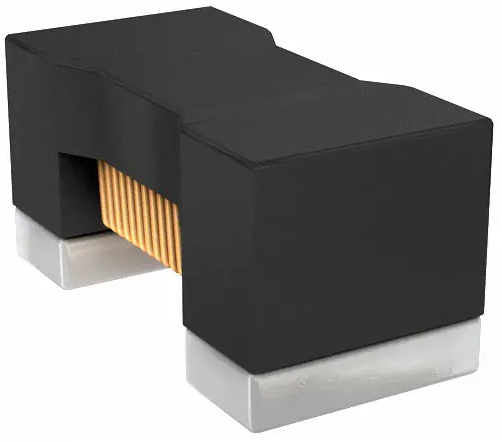 |
|
|
|
|
dramos
Advanced User
Joined: 18 Feb 2021 Status: Offline Points: 81 |
Post Options
Thanks(0)
Quote Reply
Posted: 04 Mar 2021 at 12:17am |
|
Hi Tom:
Yes you are right . We are using more and more this kind of components in our designs. Many thanks for your recommendations. Regards. David
|
|
|
|
|
IMI4tth3w
New User 
Joined: 04 Mar 2021 Status: Offline Points: 1 |
Post Options
Thanks(0)
Quote Reply
Posted: 04 Mar 2021 at 8:53am |
|
I actually just did a footprint for one of these types of inductors.
Coilcraft seems to have pretty good guidelines for footprints in their datasheets. Here's an example: https://www.coilcraft.com/en-us/products/rf/ferrite-core-chip-inductors/0603-(1608)/0603ls/ |
|
|
|
|
Tom H
Admin Group
Joined: 05 Jan 2012 Location: San Diego, CA Status: Offline Points: 5954 |
Post Options
Thanks(0)
Quote Reply
Posted: 04 Mar 2021 at 9:06am |
|
Continue to use the mfr. recommended pattern for this new package style and new terminal lead form.
Automating a software program to calculate the pad stack would need to identify a new terminal lead form and then the solder joint goal table for a 3-Tier density level. It's too late to put it in IPC-7351C and it's not in IPC-J-STD-001 yet for assembly solder joint acceptability. |
|
|
|
|
Jeromeli
Active User 
Joined: 10 Jun 2021 Status: Offline Points: 12 |
Post Options
Thanks(0)
Quote Reply
Posted: 01 Apr 2022 at 5:55am |
|
I have encountered a similar problem recently, and I am trying to solve it
|
|
|
|
|
Tom H
Admin Group
Joined: 05 Jan 2012 Location: San Diego, CA Status: Offline Points: 5954 |
Post Options
Thanks(0)
Quote Reply
Posted: 01 Apr 2022 at 10:46am |
|
You must use the Manufacturer's Recommended Pattern.
|
|
|
|
|
pem3bg
New User
Joined: 16 Aug 2023 Status: Offline Points: 1 |
Post Options
Thanks(0)
Quote Reply
Posted: 30 Jun 2025 at 6:36am |
|
Hi all, I'm trying to create footprint for an inductor like on the next picture: 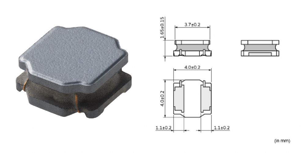
What would be the best type to use for this inductor (Chip Inductor or DFN 2 pins Inductor). I'm asking this because I want to have IPC name for this footprint and when I create footprint with both types I got different name. So what would be the best solution for this. It's Murata LQH44PN150MPRL |
|
|
|
|
Tom H
Admin Group
Joined: 05 Jan 2012 Location: San Diego, CA Status: Offline Points: 5954 |
Post Options
Thanks(0)
Quote Reply
Posted: 30 Jun 2025 at 7:36am |
|
This Murata LQH44PN150MPRL have a trapezoid pad shape.
It cannot be created in Footprint Expert, but we can build it in a CAD tool and export/import the ASCII file into FPX format. 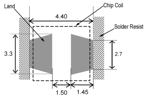 |
|
|
|
|
Post Reply
|
|
| Tweet |
| Forum Jump | Forum Permissions You cannot post new topics in this forum You cannot reply to topics in this forum You cannot delete your posts in this forum You cannot edit your posts in this forum You cannot create polls in this forum You cannot vote in polls in this forum |


 Topic Options