|
|
0603 Chip Minimum Land Pattern |
Post Reply 
|
| Author | |
SandroLanot 
New User 
Joined: 11 Feb 2015 Status: Offline Points: 13 |
 Post Options Post Options
") Thanks(0) Thanks(0)
 Quote Reply Quote Reply
 Topic: 0603 Chip Minimum Land Pattern Topic: 0603 Chip Minimum Land PatternPosted: 15 Feb 2015 at 9:18pm |
|
Guys and Gals, Good day. I am on the midst of my design, and i am planning to place 0603 resistor under the 1.0 mm pitch BGA and because of the 1 pin/1 via in the area, I am having difficulty placing them. Please help advice what is the minimum land pattern I can modify my standard 0603 so that I can fit them inside.. My current land pattern is rectangular 0.6 X 0.9 mm, with 1.4 pitch. Thanks |
|
 |
|

|
|
|
|
|
Tom H
Admin Group 

Joined: 05 Jan 2012 Location: San Diego, CA Status: Offline Points: 6074 |
Post Options
Thanks(1)
Quote Reply
Posted: 16 Feb 2015 at 8:40am |
|
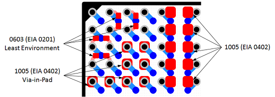
The minimum (least environment) for a 0603 pattern is 0.70 X 0.85 with a 1.0 mm pitch.
You can only put this under a 1.0 mm pitch BGA if there are unused pins in the area and you fanout your vias away from the resistor. However, you can fit a 0402 nominal resistor in-between vias. This picture is a 1.0 mm pitch BGA.
|
|
|
|
|
Post Reply
|
|
| Tweet |
| Forum Jump | Forum Permissions You cannot post new topics in this forum You cannot reply to topics in this forum You cannot delete your posts in this forum You cannot edit your posts in this forum You cannot create polls in this forum You cannot vote in polls in this forum |


 Topic Options