Terminal Lead Forms
Printed From: PCB Libraries Forum
Category: Libraries
Forum Name: PCB Libraries Guideline
Forum Description: (online edition)
URL: https://www.PCBLibraries.com/forum/forum_posts.asp?TID=3687
Printed Date: 05 Oct 2026 at 5:16am
Topic: Terminal Lead Forms
Posted By: Nick B
Subject: Terminal Lead Forms
Date Posted: 20 Aug 2026 at 11:00am
|
BGA 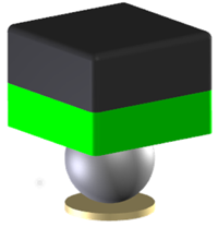 A surface mount integrated circuit packaging type that utilizes a matrix of small solder spheres (solder balls) on the underside of the component to establish external electrical connections to a printed circuit board (PCB). By replacing traditional perimeter-only leads or pins with a full-surface area array, BGAs provide drastically higher interconnect density. This configuration optimizes electrical performance through shorter internal trace paths, dramatically reducing parasitic inductance and impedance in high-speed applications. There are Collapsing and Non-collapsing BGA balls. Collapsing 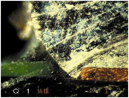 Non-collapsing 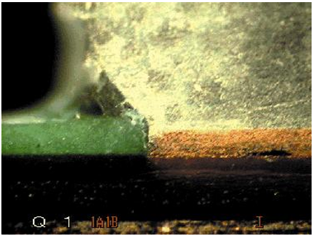 There is also a Solder Mask Defined BGA that has solder mask over the pad edges. The annular ring of the solder mask on pad is typically 0.05 mm. This technology is primarily used to secure the PCB pad to the PCB prepreg in handheld devices like cell phones. During drop tests, the solder joint between the BGA ball and the pad remains intact, but the pad could separate from the prepreg. Solder mask and prepreg are both epoxy resin (glue). The solder mask will help secure the pad to the prepreg to prevent the pad separating from the prepreg. This solder mask defined concept is primarily used on BGA pin pitches of 0.65 mm and lower, where the non-collapsing pad size is larger than the BGA ball diameter. 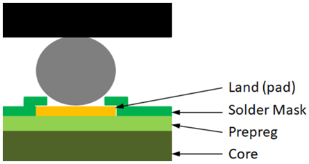 The primary reason for making the BGA pad size larger than the ball diameter is to accommodate via-in-pad technology because fine pitch BGAs cannot use the typical Dog-bone via fanout solution. Dog-bone via fanout: 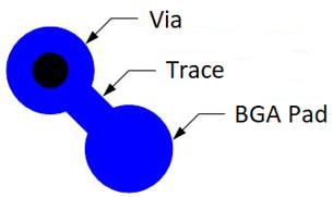 When creating dog bone fanouts for BGAs, the escape trace should be kept as wide and as short as possible. Generally, the trace is a wide as the ball width. A wider trace reduces series inductance, which is critical because the fanout forms part of the high frequency return path loop between the BGA ball, via, and internal plane. Narrow traces behave like inductors at RF, increasing impedance, degrading signal rise time, and injecting noise into adjacent balls. Via-in-Pad technology is a technique used in PCB design where the via is placed directly in the pad. This approach is commonly used in high-density interconnect (HDI) designs, especially for fine pitch BGAs. 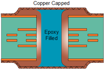 The via-in-pad (VIP) requires a separate fabrication process that includes plating, plugging and capping the hole and planarizing the capped pad to create a flat surface with no dimples. Capped pads with dimples create trapped air under the paste mask. When the PCB goes through the reflow oven, the trapped air in the pad dimple gets super-heated and blows through the solder and into the BGA ball causing a void. 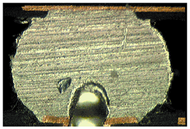 Most of the time the via-in-pad is a microvia that goes from the top layer to the first signal layer. Then buried vias connect to all the other inner layers. All BGA GND connections use microvias to Layer 2. However, PCB fabrication can now drill a hole with a 10:1 aspect ratio. A 1.57 mm thick PCB can support a via hole size of 0.15 mm. But the pad size must be 0.35 to support a 0.10 mm annular ring. This solution is good for 0.40 - 0.65 mm pitch BGAs. The free Footprint Calculator and the Footprint Expert use these tables for BGA footprint calculations. The Footprint Expert also creates high-quality BGA footprints and 3D STEP models directly from the package dimensions. 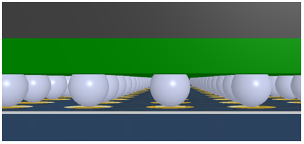 BGA Ball Materials: The BGA ball may consist of a variety of metal alloys. Some of these include balls with some lead content such as 37Pb63Sn, 90Pb10Sn, 95Pb5Sn, while others do not contain lead such as Sn96.5Ag3.0Cu0.5, Sn96.5Ag3.5, Sn-9Zn-0.003Al. It is a good recommendation to use the same alloy, in a paste form, to attach the BGA balls to the mounting substrate; however, some of the balls that do not collapse require a paste that is more conducive to reflow temperatures. Lead-free balls have a combination of tin, silver and copper. This is the replacement for the tin/lead ball. BGAs are usually assembled using the standard reflow solder processes. Rectangular or Square End Cap 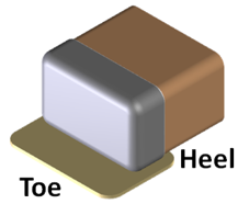 Metallized end bands or chip terminations) are the metal contact structures covering the opposing ends of passive surface mount electronic chip components. Unlike integrated circuits that use external pins, these terminal leads envelop the outer structural corners of the device to facilitate structural mounting and complete an electrical circuit. They are the standard terminal configuration for surface mount capacitors, resistors, thermistors, varistors, chokes, ferrite beads, antennas, crystals, diodes, filters, fuses, LEDs and inductors. This is the most popular lead form as chip components are usually 80% of the components on a PCB layout. Cylindrical End Cap 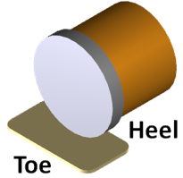 A cap-shaped, round metal contact covering the opposing ends of a cylindrical component body. Rather than using protruding wires or flat rectangular bands, MELF components utilize these flush, circular metal barrels as their electrical and mechanical mounting interfaces. This terminal style is widely utilized for high-reliability surface mount resistors, diodes, and Zener regulators in automotive, industrial, and aerospace electronics. Gullwing 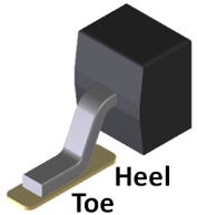 An outward-bent surface mount technology (SMT) lead shape that resembles a seagull's wing in flight. The metal leads extend horizontally from the sides of an integrated circuit (IC) package, bend vertically downward toward the circuit board, and then bend outward again to create a flat mounting foot. This flat foot provides the primary electrical and mechanical contact surface for soldering onto a printed circuit board (PCB) land pad. Gull wing leads are the dominant terminal style for highly utilized IC packages such as Small Outline Integrated Circuit (SOIC), Thin Small Outline Package (SOP), Quad Flat Package (QFP), Small Outline Transistor (SOT), Ceramic Flat Pack (CFP), Ceramic Quad Flat Pack (CQFP), Small Outline Diode (SOD) and DPAK. Outward L Lead 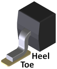 Certain small Surface Mount components, such as some SOD’s and SOTs for example, with terminal leads that can be in the form of either Gullwing or Outward flat ‘L’ depending on their dimensions. It’s important to distinguish between the two to assign the correct protrusion goals (toe, heel and side) to obtain the most reliable footprint mounting. This is how the PCBL Footprint Expert does it. 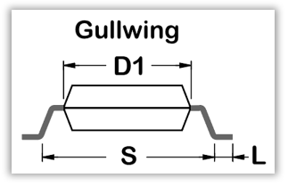 Gullwing terminals are generally for parts with relatively larger terminals and provide more heel fillet. Gullwing goals should be applied when: S min > D1 max OR (L max - L min) >= 0 .5mm 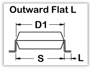 Outward Flat L terminals are generally for smaller parts and do not provide as much heel fillet. Outward Flat L goals should be applied when: S min <= D1 max AND (L max - L min) < 0.50 mm When a Gullwing change to Outward L occurs, this message will be displayed:  J-Lead 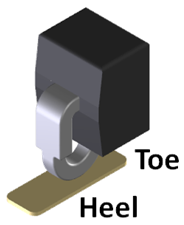 A specialized surface mount technology (SMT) component lead form that curves downward and tightly rolls underneath the package body in the shape of the letter "J". This configuration stands in contrast to Gullwing leads which extend outward. J-leads are widely used on Plastic Leaded Chip Carriers (PLCCs), memory modules, and tactile switches to reduce board footprint while maximizing mechanical compliance. Inward L Lead 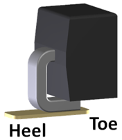 An Inward L-Lead form is a surface mount technology (SMT) component lead configuration where each terminal extends from the package body, bends downward at a right angle, and then bends sharply inward toward the center of the component body. This creates a low-profile, right-angle connection footprint that sits entirely underneath the perimeter of the device. It is primarily utilized on Small Outline L-Bend (SOL) packages and high-density ribbon assemblies to maximize available circuit board area. Side Concave 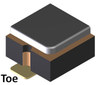 A specialized surface mount technology (SMT) terminal design where the conductive contact pad curves inward toward the body of the component, forming a scalloped indentation or semicircular castellation along its edge. This design is primarily used on dense passive components like side-concave chip resistor arrays, multi-layered ceramic capacitor (MLCC) arrays, and edge-mounted castellated sub-modules (such as Wi-Fi/Bluetooth breakout boards) Corner Concave 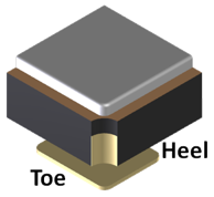 A surface mount component termination style where the conductive pads form scalloped, crescent-shaped vertical castellations directly on the outside corners of the device body. This configuration is most prominently featured on surface mount quartz crystal oscillators, clock generators, and specialized square filter modules. Flat No-Lead Side 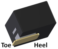 A PCB Flat No-Lead Side terminal lead (commonly categorized under flat, no-lead side terminations) refers to the perimeter signal pads found on Bottom Termination Components (BTCs). These are used on Quad Flat No-Lead (QFN) and Dual Flat No-Lead (DFN) packages. The contacts do not project from the package sides; instead, they exist as flat metalized lands on the bottom face that terminate flush with the outer cut edge of the component wall. Flat Lead 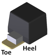 A surface mount or through-hole termination style where the component pins consist of flat, unbent, thin metal strips extending horizontally or vertically from the package body. Unlike round wire leads or pre-formed Gullwing leads, flat leads are completely linear and planar. They are primarily utilized on high-current surface mount inductors, flat-pack aerospace ICs, current-sense resistors, and planar transformers. Under Body Outward L 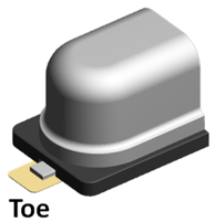 A lead variant where the pins exit from the bottom or lower edge of the component casing, bend outward, but remain entirely hidden beneath the perimeter outline of the component package. Unlike standard Gullwing leads which extend well past the sides of a chip, or Inward L-Leads which hook back inward beneath the component frame, the Under-Body Outward L lead steps outward away from the package center but terminates before exiting the package bounds. It is most frequently found on Aluminum Electrolytic Capacitors, Crystal Oscillators, heavy shielded power inductors, and specialized SOT sub-packages. Inward Flat Ribbon L 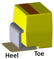 A specialized surface mount technology (SMT) lead configuration that combines the low-inductance, flat cross-section of a flat-ribbon lead with the space-saving geometry of an inward L-bend. Instead of extending outward from the component body like a standard flat ribbon lead, the lead extends downward and then bends sharply at a right angle toward the center of the component body. This ensures the entire flat contact foot is tucked cleanly beneath the device perimeter. Used for Capacitors, Inductors, Diodes, LEDs, Chokes, Ferrite Beads, and Filters. Land Grid Array/Bottom Only 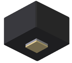 A surface mount connection interface where the component features a grid of flat, coplanar metal pads on its bottom surface instead of protruding pins or solder balls. Electrical and mechanical connection to the PCB is established via a matching pattern of landing pads and an ultra-thin layer of solder paste, or through a mechanical socket. This architecture is widely used for high-performance processors, complex field-programmable gate arrays (FPGAs), wireless modules, and high-density sensors. Column Grid Array 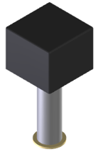 An advanced high-density surface mount packaging interface. Instead of utilizing spherical balls like a standard Ball Grid Array (BGA), a CGA utilizes an array of tall, cylindrical high-temperature solder columns or copper-reinforced posts that stand vertically on the underside of the component package. This termination style is highly specialized and explicitly preferred for large-body integrated circuits (such as space-grade FPGAs, processors, and telemetry modules) operating in harsh environments where extreme thermal fluctuations and severe mechanical vibration are constant. Flat Lug Lead (DPAK Tab) 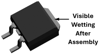 A large, heat-dissipating backside drain tab of a DPAK (TO-252) surface-mount package into a dedicated flat, surface-mounting contact terminal. It serves as the primary path for drawing destructive heat away from the silicon die and distributes it directly into the copper planes of the printed circuit board. In standard power MOSFETs, this extended tab functions as the high-current electrical connection for the Drain terminal. Avoid applying a 1:1 ratio of solder paste to the flat lug pad area. Industry guidelines from manufacturers like onsemi recommend a windowpane or checkerboard stencil pattern covering roughly 60% of the tab area. This prevents component floating, misalignment, or "tombstoning" from excess solder. The Nominal Toe value is 0.35 mm and must have visible wetting after assembly. The Side and Heel values are very small and set to 0.03 to maintain alignment and prevent skewing. However, some voltage regulator DPAK devices produce additional heat and the manufacturer recommended pattern for the thermal pad size should be taken into consideration. To maximize heat transfer from the flat lug lead, stitch multiple thermal vias into the pad connecting to inner or bottom-layer ground/power planes. Due to the massive heat-sinking nature of the extended tab, hand-soldering requires a large thermal mass iron, a pre-heating hot plate, or a secondary heating source to ensure proper solder flow under the heel of the component. Through-Hole 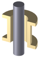 Through-hole leads rely on mechanical insertion through the substrate. Pre-forming the leads is a critical manufacturing step designed to establish a consistent component standoff height, provide strain relief, and mechanically lock the component to the board prior to wave or selective soldering. 
 The Footprint Expert automates footprints to perfection. Professional, detailed, and accurate parts - all built consistently with identical rules, regardless of how many people are involved in your library development. Get your FREE Footprint Calculator or Footprint Expert Evaluation License: https://www.pcblibraries.com/Register" target="_blank rel="nofollow" - https://www.PCBLibraries.com/Register Call us - 847-557-2300 ------------- Stay connected - follow us! https://twitter.com/PCBLibraries" rel="nofollow - X - http://www.linkedin.com/company/pcb-libraries-inc-/" rel="nofollow - LinkedIn |