Footprint Too Small For Silkscreen Outline
Printed From: PCB Libraries Forum
Category: PCB Footprint Expert
Forum Name: Options
Forum Description: the foundation of Footprint Expert's CAD LEAP Technology
URL: https://www.PCBLibraries.com/forum/forum_posts.asp?TID=3623
Printed Date: 26 Jun 2026 at 2:13am
Topic: Footprint Too Small For Silkscreen Outline
Posted By: Tom H
Subject: Footprint Too Small For Silkscreen Outline
Date Posted: 08 Mar 2026 at 12:16pm
|
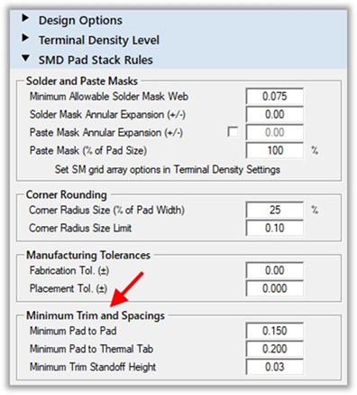
Question: How does the silkscreen spacing option consider
pads are too close? Example of a trimming rule: the Calculator trims pad
sizes for you when they fail to meet the specifications in Rules. The
default values we use are all considered best industry practice. Note: pad clearances are not guaranteed for FP Designer footprints
and there are no warnings.
The clearance of the silkscreen to the body and any pads is set in the Drafting > Silkscreen options. The silkscreen is automatically trimmed, if required, to meet these values.
There is a hard-coded minimum silkscreen line length of 3
silkscreen line widths. Any silkscreen line segment less
than this length is removed to avoid the appearance of ‘specks’ on a PCB.
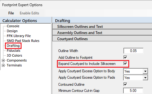
Here is a 0603 chip capacitor that has enough pad-to-pad spacing to allow a silkscreen line. This silkscreen outline length exceeds 3 line widths.
Here is a 0603 chip capacitor that violates the pad-to-pad spacing to allow a silkscreen line. The silkscreen outline wraps around the pads and the courtyard outline is pushed out to include the expanded silkscreen outline.
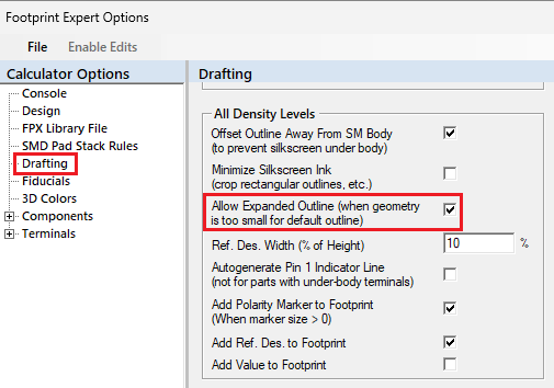
You have options to turn off the silkscreen outline if the pattern is too small to create one.
You can also turn off the courtyard excess for including the
silkscreen outline.
------------- Stay connected - follow us! https://twitter.com/PCBLibraries" rel="nofollow - X - http://www.linkedin.com/company/pcb-libraries-inc-/" rel="nofollow - LinkedIn |