
|
|
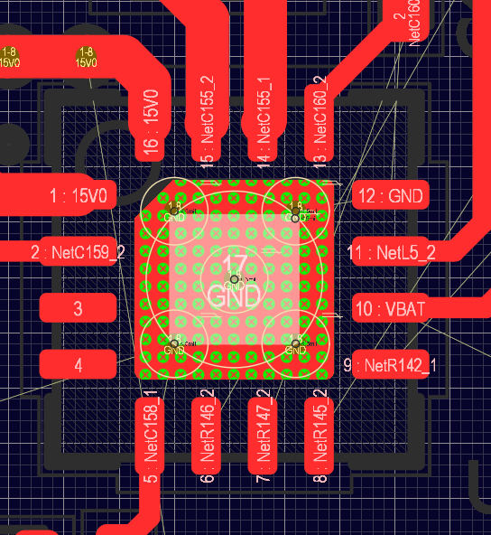
Small Pad with Larger Copper Shape |
Post Reply 
|
| Author | |
Nick B 
Admin Group 

Joined: 02 Jan 2012 Status: Offline Points: 2110 |
 Post Options Post Options
 Thanks(0) Thanks(0)
 Quote Reply Quote Reply
 Topic: Small Pad with Larger Copper Shape Topic: Small Pad with Larger Copper ShapePosted: 2 hours 44 minutes ago at 8:44am |
ANSWER: The answer is simple. Chamfered Thermal Pads in a corner by Pin 1 are not 'Flash' apertures. They are Copper Polygon Shapes and are drawn and not flashed. To make a thermal pad a Flash Aperture (a normal pad), remove the corner chamfer. |
|
 |
|

|
|
|
|
|
Post Reply
|
|
| Tweet |
| Forum Jump | Forum Permissions You cannot post new topics in this forum You cannot reply to topics in this forum You cannot delete your posts in this forum You cannot edit your posts in this forum You cannot create polls in this forum You cannot vote in polls in this forum |


 Topic Options