

|
|
SODF OR DFN |
Post Reply 
|
| Author | |
dramos 
Advanced User 
Joined: 18 Feb 2021 Status: Offline Points: 103 |
 Post Options Post Options
 Thanks(0) Thanks(0)
 Quote Reply Quote Reply
 Topic: SODF OR DFN Topic: SODF OR DFNPosted: 15 Apr 2026 at 10:23am |
|
Hi Tom and Team,
I was working in this SOD-523 diode, onsemi part number RB751S40T1G . Suddenly, I had a doubt with a value because the length of the pin is 0.30mm REF, I was thinking to use +/-0.05mm of tolerance but I said to my self: "how PCBFE resolve this question? and I've gone to the Parts area and bingo! it is ready to download. After downloading I opened it and It was not similar to a SOD-523, it seems more a DFN component.  Could we consider this kind of components a DFN and why? My first impression has been: the footprint is no correct but then... and why not? I attached the downloaded file as well. My component was more "traditional"  I attached as well my component fpx Anyway I am not very happy with my footprint and as now we have a new feature where we can modify the corners of a footprint when the pad is rounded rectangle or chamfered pad. 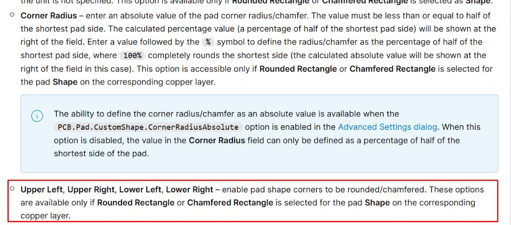 Using this feature I created the inner corners of the component squared and outer corners rounded. the inner corners are under the component and perhaps are more close to s DFN... What's your opinion? 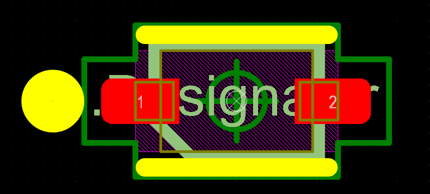 Thanks for your comments, they are always really appreciated. Regards, David
|
|
 |
|

|
|
|
|
|
Tom H
Admin Group 

Joined: 05 Jan 2012 Location: San Diego, CA Status: Offline Points: 6098 |
Post Options
Thanks(0)
Quote Reply
Posted: 15 Apr 2026 at 10:47am |
|
This package is definitely a SODFL package.
A DFN is a BTC package where the terminal lead are completely under the package body. DFNs do not have terminal leads that protrude outside the package body. SODFL: 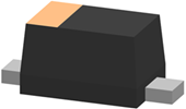 DFN: 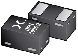 |
|
|
|
|
dramos
Advanced User
Joined: 18 Feb 2021 Status: Offline Points: 103 |
Post Options
Thanks(0)
Quote Reply
Posted: 15 Apr 2026 at 11:49pm |
|
Dear Tom and Team,
Yes, I thought the same about SODF and DFN. So I consider that the footprint I created is correct. In the other hand, it is my question about the shape of the internal corners of the pad. On our company, when we create a footprint we build it with Nominal density option and Most density option. The program allows to do it in a very fast and easy way. In both cases, the value Side and Heel is 0.00. It could be similar to the value 0.00 that we have in the Periphery parameter on a DFN. Furthermore, there are some SODF components where the lead is below the body, for example the mentioned RB751S40T1G. Yesterday, when I saw the component that I downloaded I started thinking that perhaps it had sense and It could be done using the new features that Altium developed. I know that it could be a crazy idea, but I would like to start this discussion with you because in PCBFE you have a big and long knowledge. You've been involved in footprints for decades. In my company there is not a dedicated librarian to share with him this kind of ideas. Anyway, thanks for your comments. david |
|
|
|
|
dramos
Advanced User
Joined: 18 Feb 2021 Status: Offline Points: 103 |
Post Options
Thanks(0)
Quote Reply
Posted: 17 hours 35 minutes ago at 10:56pm |
|
Hi Team,
I am coming again with the same idea. I've been working now with a SOD-323F diode from DIODES. 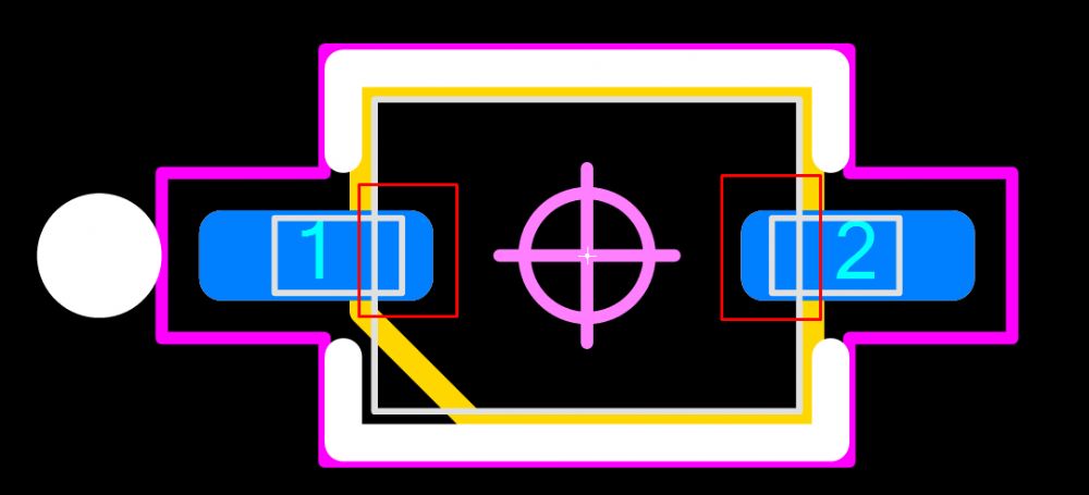 I would like to read your comments, not only Tom and Nick, about what do you think about the idea of modify the radio of the inner corners of the pad or even making them completely squared. Here my reasoning is similar to thermal tabs, we build them completely squared to fit them perfectly on the pad. Here I believe that if we decrease the inner radio perhaps we could make the pad even smaller. Now there is an aprox. distance of 0.12mm between the center of inner side of the pin and the center of the inner side of the pad. But this distance is not real because the corners are rounded and if the component is moved this distance to the right or to the left the corners of the pin are going to be outside the pad. The possibility of this movement is real. There is a lot of space between the pin and the external border of the pad. I believe that could be a reasonable thought. Looking forward to hearing your comments. david
|
|
|
|
|
Tom H
Admin Group
Joined: 05 Jan 2012 Location: San Diego, CA Status: Offline Points: 6098 |
Post Options
Thanks(0)
Quote Reply
Posted: 7 hours 28 minutes ago at 9:03am |
|
The terminal leads for DFN packages are 100% under the package body. The Diodes SOD323F is in the SODFL component family. The SODFL terminal leads are under the body and also protrude beyond the package body. 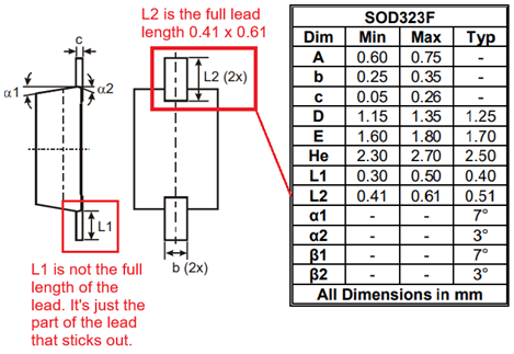 |
|
|
|
|
dramos
Advanced User
Joined: 18 Feb 2021 Status: Offline Points: 103 |
Post Options
Thanks(0)
Quote Reply
Posted: 2 hours 44 minutes ago at 1:47pm |
|
Hi Tom,
Thanks for your fast reply!!! We are in the same page about the type of the diode. The main difference between both types is that the SOD has Toe, Heel and side values for some density levels. I would like your idea to mix both on SOD, from the Toe add the solder joint and from the Heel make it completely squared without radio on corners because it is under the body. Regards, david
|
|
|
|
|
Tom H
Admin Group
Joined: 05 Jan 2012 Location: San Diego, CA Status: Offline Points: 6098 |
Post Options
Thanks(0)
Quote Reply
Posted: 2 hours 11 minutes ago at 2:20pm |
|
Under body DFN terminal leads have a Periphery pad calculation based on the terminal lead tolerances so that the resulting pad stack can handle the terminal lead in the maximum material condition.
In this case the pad stack would have the same shape as the terminal lead - rectangle. 90% of the solder joint strength is under the Flat Lead. But assembly would like to see visible wetting in the toe for visual inspection. The Toe, Heel and Side are there to allow the solder under the terminal lead to flow outward during reflow. All bottom terminal lead pad stacks are slightly larger than the terminal lead to allow the lead to settle into the solder paste during reflow. Making the pad size the same as the terminal lead size is not recommended. But since the pad stack periphery is slightly larger than the terminal lead, the pad shape needs to be the same as the terminal lead as there is no room for rounded rectangle pad shape without exposing the terminal lead. |
|
|
|
|
Post Reply
|
|
| Tweet |
| Forum Jump | Forum Permissions You cannot post new topics in this forum You cannot reply to topics in this forum You cannot delete your posts in this forum You cannot edit your posts in this forum You cannot create polls in this forum You cannot vote in polls in this forum |


 Topic Options