

|
|
SMD Pad Stack Rules |
Post Reply 
|
| Author | ||||||||||||||||||||||||||||
Nick B 
Admin Group 

Joined: 02 Jan 2012 Status: Offline Points: 2076 |
 Post Options Post Options
 Thanks(0) Thanks(0)
 Quote Reply Quote Reply
 Topic: SMD Pad Stack Rules Topic: SMD Pad Stack RulesPosted: 15 Aug 2026 at 11:00am |
|||||||||||||||||||||||||||
|
Pad Stack Rules will globally define the rules for every footprint created in the Surface Mount Calculators. These rules are not used for custom FP Designer footprints because the user manually defines every pad stack in custom parts. Custom footprints always use the component manufacturer recommended pattern and pad sizes because there are no standard recommendations or guidelines for unique packages and their related footprint patterns. The default values are best known practice, but users can edit any value for their PCB library requirements. 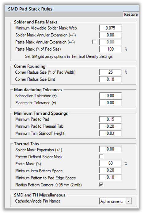 Solder and Paste Masks Solder Mask Note: Solder mask is an epoxy coating that protects the circuit from corrosion and electrical shorts. It also provides electrical insulation that allows higher voltage traces to be placed nearer to each other. Most importantly, the solder mask keeps the solder on the pads, as opposed to flowing onto traces, planes, or empty board space. This reduces the likelihood that solder will form bridges (unintended connections) from one element to another. Solder masks are critical for wave soldering, which is a mass production technique. Solder masks also make hand soldering faster, easier, and more accurate. a. Minimum Allowable Solder Mask Web - 0.075 or 0.10 This rule is for PCB fabrication. The solder mask stencil must have a minimum 0.075 mm between pads. Anything less than that is not manufacturable. When the solder mask web violates the minimum value, Footprint Expert will automatically gang the solder mask into a solid block. If you provide Gerber data with a solder mask web less than 0.075 mm to fabrication, they will automatically gang mask the row of pads for you, and not tell you. If you provide 1:1 scale solder mask to fabrication, they will swell the mask to meet their fabrication tolerance for their solder mask application. Fabrication CAM tools will alert the operator of all solder mask webs less than 0.075 and the operator will gang mask all solder mask areas that violate the minimum solder mask web. b. Solder Mask Annular Ring Expansion - typically between 0.05 - 0.075 Some PCB designers use a solder mask expansion between 0.05 - 0.075 because they use that as a visual for placing reference designators on a final part placement. Silkscreen Legend Ink should not be in an exposed solder mask area. If you place silkscreen legend in a solder mask free area in your PCB layout, the fabrication process will automatically trim the silkscreen legend away from the free solder mask area. But many PCB designers leave the solder mask 1:1 scale of the pad and allow the PCB fabrication shop to automatically swell all solder mask features to meet their solder mask registration tolerance. c. Paste Mask (% of Pad Size) - 100% Normally, paste mask on pads is 1:1 scale but this option allows the user to increase or reduce the amount of Paste Mask on a pad. 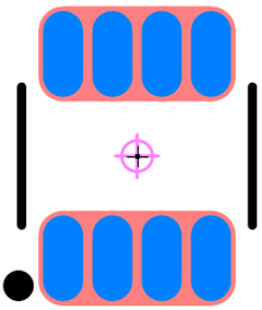 d. Gang Solder Mask When the Solder Mask Annular Expansion rule is violated, Footprint Expert will automatically Gang Mask the entire row. This image illustrates an Oblong pad shape Gang Mask 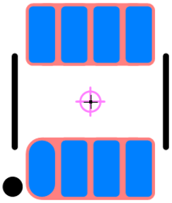 This image illustrates a Rounded Rectangle pad shape with Pin 1 Oblong Gang Mask e. RF Design Note For RF, microwave and high frequency controlled impedance traces, solder mask should be removed from above the transmission line. The solder mask alters the dielectric environment by replacing air (Dk ≈ 1) with mask resin (Dk ≈ 3-4), increasing effective Dk, adding loss, and disturbing the EM field distribution that defines the line's impedance. Mask thickness and moisture absorption further introduce variability. To maintain stable impedance and minimize RF loss, specify a solder mask keep-out over all RF microstrips, antennas, and matching network traces. Corner Rounding a. Corner Radius Size (% of Pad Width) - 25% The 25% value is applied to every corner, that is equivalent to 50% of the pad width. b. Corner Radius Size Limit - 0.10 The 0.10 default value sets the limit on the corner radius. Some component manufacturers recommended solder patterns indicate a 0.05 mm corner radius. The corner radius size limit is totally up to the PCB designer or CAD librarian. There is no recommended Standard for this radius limit. Some companies use a 0.15 - 0.20 Corner Radius Limit. Any value above 0.20 is excessive. Corner Radius Note: Some people say that rounded rectangle pad shape is best for lead free solder. This is a myth, as all pad shapes are OK with lead free solder. IPC has recommended Oblong pad shape since the release of IPC-SM-782 in March 1987. The 782 Standard had both text and graphic illustrations. The text referred to Oblong (or Full Radius) pad shape but the images portrayed Rectangle Pad Shape. This was confusing to the reader of the Standard. Most component manufacturers recommended patterns for surface mount parts illustrate Rectangular pad shape. The Rounded Rectangle Pad Shape is a compromise between the world standard Oblong and the component manufacturer Rectangle. Also, it is important to note that paste mask stencil aperture openings are laser cut with rounded corners. It makes sense to have the pad shape match the paste mask stencil aperture shape. 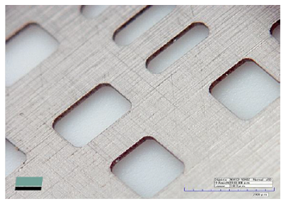 When the PCB goes through a reflow oven, the paste mask tends to gravitate toward the terminal lead and away from the pad corners. It doesn't make sense to have rectangular pad shapes with no solder in the pad corners. Here is a photo of both lead and lead-free solder with no solder in the corners. 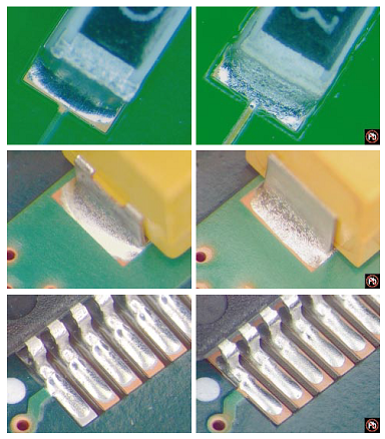 Manufacturing Tolerances Manufacturing Tolerances Note: Manufacturing tolerances have existed in the IPC mathematical model for surface mount pad size calculation since 1987. The Fabrication Tolerance was used to compensate for the etching process. But in the 1990's, the fabrication shops started to swell the outer layers to compensate for their etch back tolerances so that they could deliver pad sizes and trace widths the same size as the original Gerber data. But there is also an issue with the subtractive process where the etch acid gets slightly under the photo resist and creates a trapezoidal effect in the trace and pad. IPC-7351 uses a 0.05 mm fabrication value in the pad size math to compensate for this subtractive process. The average copper thickness on the outer layers is ½ oz. or 0.017 mm. The acid under photo resist undercut value is only a small percentage of that. Basically, the Fabrication Tolerance added to the pad size calculation is no longer applicable. 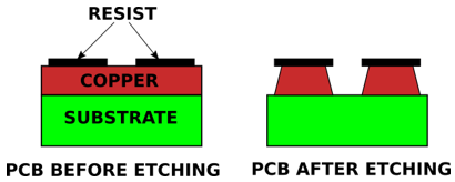 The Assembly Tolerance used in the IPC-7351 mathematical model for pad size calculation is 0.025 and established in 1987. This value was to compensate for the assembly machine placement accuracy. Today's advanced assembly machines place components with a 0.01 accuracy or less. The Assembly tolerance added to the pad size calculation is no longer applicable today. When IPC developed the solder joint goals for IPC-7351, side goals for fine pitch semiconductor packages had to be set at negative values to compensate for the robust manufacturing tolerances. IPC-7352 turned off the manufacturing tolerances and updated every negative value in the Terminal solder joints to 0.00. By turning off the manufacturing tolerances and changing all negative solder joint goals to 0.00, the pad length & width size is only affected by +/-0.05.
IPC-7352 changed the Fab & Assy Tolerances:
Minimum Trim and Spacing a. Minimum Pad to Pad - 0.15 The minimum pad to pad rule is intended for surface mounted parts. When the pad spacing violates this rule, Footprint Expert will automatically trim the pad to enforce this rule and an error message will be created that looks like this: 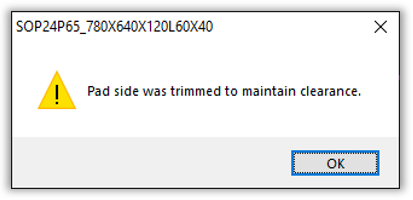 The value of 0.15 is arbitrary and not a hard-coded standard. The minimum pad to pad spacing rule should never violate your minimum PCB clearance rule. If your PCB layout is using a minimum trace/space rule of 0.20 mm then you should set the minimum pad to pad rule to 0.20. Also, if you wanted to insure a 0.08 minimum solder mask web and your solder mask swell is 0.05 then change the value to 0.18. If the minimum pad to pad is 0.15 and the pads violate that rule, the Gang Mask feature will kick in and mask the entire row. b. Minimum Pad to Thermal Tab - 0.20 The minimum pad to thermal rule is primarily established by the majority of component manufacturer's recommended patterns and not any industry Standard. If the thermal pad is too big and violates this rule, the pads will be trimmed, and a warning message will be created that looks like this: 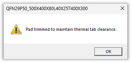 c. Minimum Trim Standoff Height - 0.03 The minimum stand-off is the A1 package body bottom to PCB space dimension in gull wing packages. 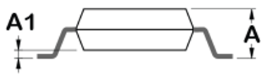 The default "minimum" value of 0.03 mm will only trim pad Heel under the component package if the A1 value is less than 0.03. The main purpose for pad trimming under low profile packages is to eliminate paste mask from touching the plastic body during reflow. The pad Heel is an important part of the gull wing solder joint, but if the Heel pad is under a low profile package, the solder on the pad Heel is pushed out by the weight of the package creating excess solder. IPC-J-STD-001 mentions in table 7-7 Dimensional Criteria - Flat Gullwing Leads. Note 4: Solder should not extend under the body of surface mount components whose leads are made of Alloy 42 or similar metals. Thermal Tabs a. Solder Mask Expansion +/- 0.00 Typically, the thermal tab solder mask is 1:1 scale of the pad size. It's OK for the fabrication solder mask tolerance to be +/- 0.05 that could result in the solder mask creeping over the thermal pad. The minimum paste mask aperture is 0.10 mm from the edge of the thermal pad. Most component manufacturers recommend a 1:1 scale solder mask on thermal pads. b. Pattern Defined Solder Mask - on/off check box The default setting for this feature is turned off because the user must accept the responsibility for turning it on. The solder mask defined thermal pad places solder mask in-between the paste mask apertures, basically damming in the paste mask from flowing. The IPC-7093A describes all the benefits of this feature. Ability to add vias in the solder mask area and the paste mask will not flow down the via hole. This could potentially save on fabrication costs to avoid via plugging to stop the flow of paste mask into the via hole. 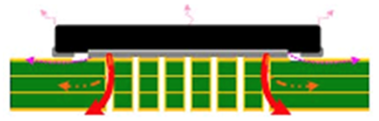 This image provides some basic values for defining a solder mask defined thermal pad. 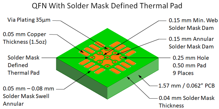 This image illustrates a 0.10 mm paste mask stencil thickness for the image above. 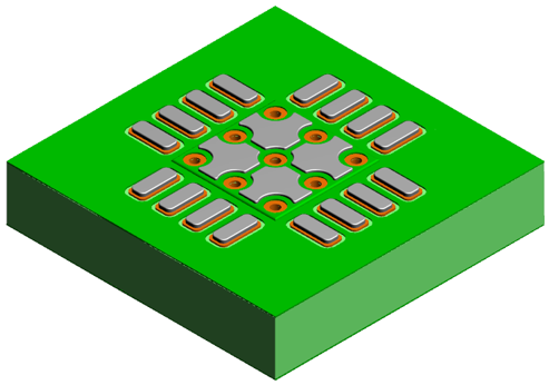 Because the paste mask is dammed in by solder mask, this reduces paste mask voiding because the solder has nowhere to flow. The amount of voiding post reflow should not exceed 25% per IPC-A-610. Voiding occurs when the thermal pad is not solder mask defined. 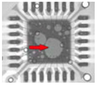 c. Paste Mask % - 60% The default setting is 60% paste mask coverage. IPC-7093A figure 3-10 recommends that the stencil design provide 60 - 70% solder paste coverage on the thermal pad area. d. Minimum Intra-Pattern Pattern Space - 0.20 The default setting for this feature is 0.20 mm. It is important to have a minimum stencil aperture spacing to increase the stencil web strength. This will make the stencil last longer and work better. e. Minimum Pattern to Pad Edge Space - 0.10 The default setting for this feature is 0.10 mm. This setting works OK up to 70% paste mask coverage. If you need 80% paste mask coverage, you will need to set this value to 0.00 to allow paste mask to extend to the edge of the pad. If you keep the 0.10 paste to pad edge and have 80% paste mask coverage, the checkerboard pattern will turn into a single aperture. 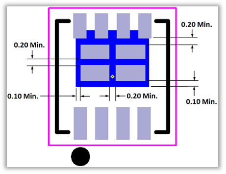 If you use the solder mask defined thermal pad feature and intend to place vias in-between the paste mask you need to figure out the via hole size and add 0.10 for the minimum pattern space. Example: if the via hole size is 0.20 + 0.10 clearance for the solder mask web, then the thermal tab minimum pattern space should be set to 0.30. Or you can move the calculator part to FP Designer and edit the pad stack paste mask to set the aperture size and spacing. Note 1: The Solder Mask and Paste Mask aperture opening are the same size and location. Note 2: 9 vias provide the maximum thermal relief for most packages with thermal tabs. 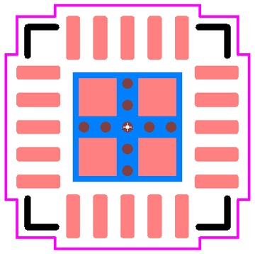 SMD and TH Miscellaneous Cathode/Anode Pin Names - Alphanumeric or Numeric The default setting is Alphanumeric and produces pin names A & C. This setting is primarily used for schematic symbols that support Alphanumeric pins. The preferred pin label assignments for Diodes and LED's are C and A for Cathode and Anode. This avoids making a mistake between the schematic symbol and the CAD library. But if you use numeric pin names on these polarized devices, you must make sure that the schematic symbol pins 1 & 2 match the PCB footprint pins 1 & 2. You can also rename Diode and LED pins to any alphanumeric value to match the schematic. |
||||||||||||||||||||||||||||
 |
||||||||||||||||||||||||||||

|
||||||||||||||||||||||||||||
|
||||||||||||||||||||||||||||
|
Post Reply
|
|
| Tweet |
| Forum Jump | Forum Permissions You cannot post new topics in this forum You cannot reply to topics in this forum You cannot delete your posts in this forum You cannot edit your posts in this forum You cannot create polls in this forum You cannot vote in polls in this forum |


 Topic Options