
PCB Libraries Forum Homepage
Forum Home Forum Home > Libraries > PCB Library Construction Guidelines > PCB Libraries Guideline
  New Posts New Posts RSS Feed - Pad Shapes
  FAQ FAQ  Forum Search   Events   Register Register  Login Login

Pad Shapes

 Post Reply Post Reply
Author
Message
Nick B View Drop Down
Admin Group
Admin Group
Avatar

Joined: 02 Jan 2012
Status: Offline
Points: 2070
Post Options Post Options   Thanks (0) Thanks(0)   Quote Nick B Quote  Post ReplyReply Direct Link To This Post Topic: Pad Shapes
    Posted: 15 Aug 2026 at 11:00am
Surface Mount

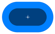
Oblong
Recommended by IPC-7351

D-Shape
Recommended by some component manufacturers

Rectangle
Recommended by most component manufacturers

Square
Used on Land Grid Arrays (LGA)

Rounded Rectangle
Recommended by assembly shops for better stencil release; the default corner radius is 0.10 mm

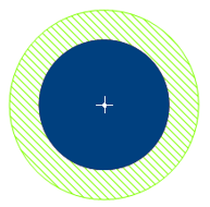
Round
Used on Grid Arrays (BGA. CGA and LGA)


Through-hole

Square
Used on Pin 1 for Polarity on Diodes and Polarized Capacitors

Round
Used on all through-hole parts

Rounded Rectangle
Used on Pin 1 for Polarity on Diodes and Polarized Capacitors


FP Designer Surface Mount
  • FP designer includes all calculator pad shapes. These are the custom pad stacks available in FP Designer.
  • Rectangle and square pad shapes can be chamfered in 2 corners on the Top, Bottom, Left and Right sides.

Top Chamfer
Chamfered on one Corner in Upper Left, Lower Left, Upper Left, Upper Right.

Upper Left

Chamfered Lower Left with Radius Corners


FP Designer Through-hole

Slotted Hole


Non-Plated Hole


Offset Slotted Hole


Chamfered Square


Round Hole with Oblong Pad


Chamfered Rectangle with Offset Hole


Stay connected - follow us! X - LinkedIn
Back to Top
 
Back to Top
 Post Reply Post Reply

Forum Jump Forum Permissions View Drop Down


This page was generated in 0.078 seconds.