|
|
Manufacturer Recommended Patterns |
Post Reply 
|
| Author | |
Nick B 
Admin Group 

Joined: 02 Jan 2012 Status: Offline Points: 1974 |
 Post Options Post Options
") Thanks(0) Thanks(0)
 Quote Reply Quote Reply
 Topic: Manufacturer Recommended Patterns Topic: Manufacturer Recommended PatternsPosted: 05 Jan 2025 at 5:20pm |
|
The misconception that simply using the manufacturer recommended pattern will keep you safe is enough to get you in serious trouble, and over time, create mayhem in your CAD library. You need much more than the recommended pattern for a reliable PCB design! Most component manufacturers provide recommended solder patterns in their datasheets, but there are two major issues you need to consider:
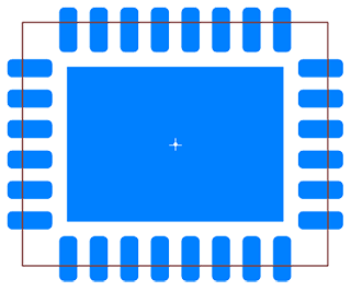
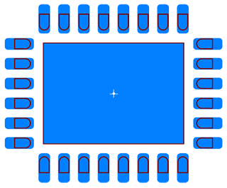
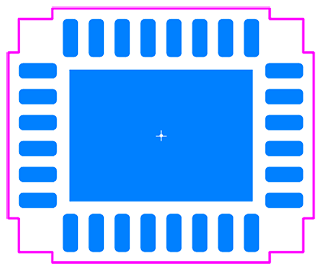
Here is a Manufacturer Recommended Pattern with rounded rectangle pad shape. All component manufacturers (except Texas Instruments) recommended rectangle pad shape. However, paste mask stencil apertures are laser cut with rounded corners.  This is obviously missing the six critical drafting outlines. Traditionally, these have been manually created with a plethora of inconsistent rules that get adjusted over time:
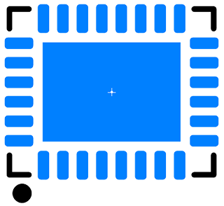
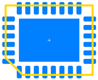
It takes more time to manually add all the necessary Drafting Outlines than it does to create the Manufacturer Recommended Pattern, and these are just as important as the pattern itself! We offer technology that automatically generates these from package dimensions! All drafting outline widths and spacings are defined in your personal master Options file. This guarantees consistent quality throughout your entire CAD library. You can also turn off any drafting outline that you do not want in your CAD library, but easily “bring it back” if you decide later that you need it! This is your end goal, read on for details how to reach it: 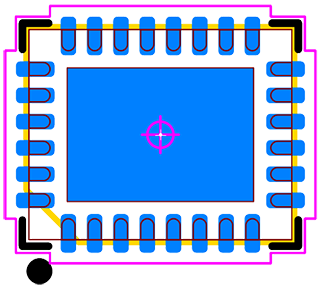 The drafting outlines are important in the following ways:
The Footprint Expert autogenerates all these drafting outlines from the same component dimensions used to calculate and generate the component footprint. It comes with pre-defined rules commonly used, which can be easily customized to your specific needs. The Footprint Expert allows you to modify this set of rules, then batch a new library in seconds with the modified rules! The CAD tool interface in Footprint Expert allows you to choose the layer assignment for each drafting outline. Here is a sample layer assignment for a CAD tool. Using the package dimensions, Footprint Expert also creates a high-quality 3D STEP model.   Create IPC or FED compliant footprints using package dimensions and your personal Options for pad stack rules, drafting outlines and solder joint goals.
Welcome to the future of PCB design with the PCB Footprint Expert software - it is precision, speed, and innovation at your fingertips. Get the ultimate solution for creating precise, effortless, error-free PCB footprint solder patterns! Register on the PCB Libraries website and request your free evaluation license and web-based demo today! Get your FREE Footprint Calculator or Footprint Expert Evaluation License: Call us - 847-557-2300 |
|
 |
|

|
|
|
|
|
Tom H
Admin Group

Joined: 05 Jan 2012 Location: San Diego, CA Status: Offline Points: 5985 |
Post Options
Thanks(0)
Quote Reply
Posted: 4 hours 54 minutes ago at 10:46am |
|
Another interesting observation on manufacturer recommended patterns is that most of the recommended patterns do not use min/max technology for pad stack calculation.
It seems the many component manufacturers use Nominal package dimensions and simply add a Toe, Heel and Side solder joint. This is typically true for most chip components. IPC-7351 and 7352 use a min/max mathematical model. This includes the component package and terminal tolerances. The resulting pad stack pattern is capable of handling accurate assembly attachment when the component package comes in the minimum, nominal or maximum material condition. The main point is that many component manufacturers provide robust package and terminal tolerances, but the recommended pattern that they publish in their datasheets will not accommodate a component that is delivered in the minimum or maximum material condition. This issue sheds light on the accuracy or necessity of component mfr. tolerances. Are they realistic? And if so, why don't the publish patterns that will accommodate min/max condition components? Here is an example of a 1206 capacitor from Murata. Part Number: GRM31CC72A475KE11L Case Code: GRM31C Here are the package dimensions. every value has a 0.30 mm tolerance. 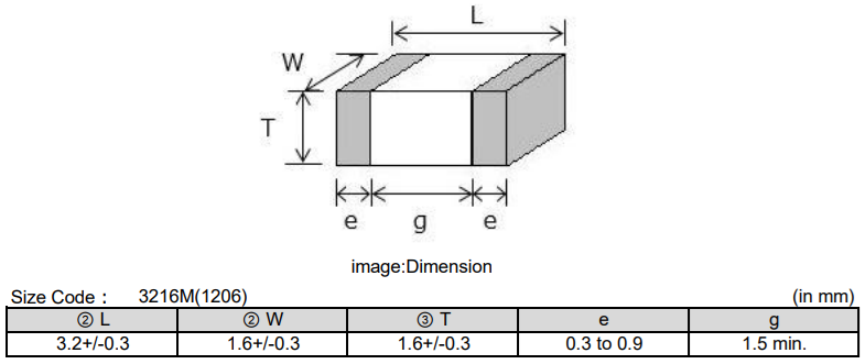 Here is the manufacturer recommended footprint: 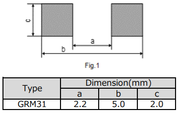 Here is the footprint using Nominal Package dimensions and the mfr. pattern. Notice the terminals are off the pad stack. No Heel. 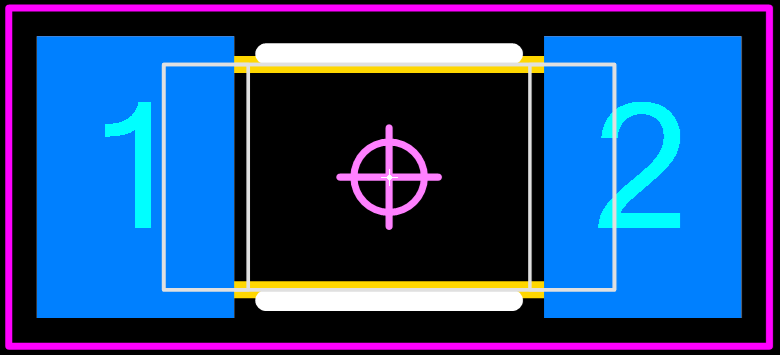 Here is the minimum package material condition according to the tolerances and the mfr. recommended pattern. The terminals are way off the pad stack. No Heel. 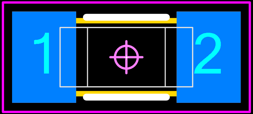 Here is the maximum package material condition according to the tolerances and the mfr. recommended pattern. No Heel and minimum Side fillet. 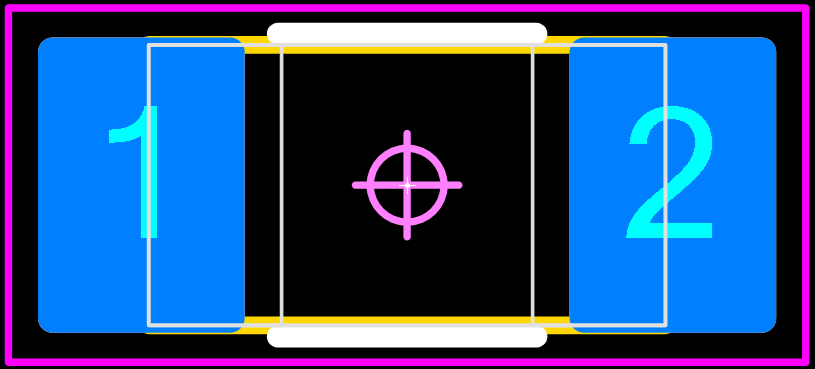 The mfr. recommended pattern does is not compatible when the component package comes in minimum, nominal or maximum material condition. Try this out with your chip manufacturer recommended patterns to ensure that the pad stacks will accommodate a package in all material conditions. If not, the package and terminal tolerances could be too robust. The FED Standard 'Volume 18' for The New Proportional Land Dimensioning Concept highly recommends not to use any mfr. package tolerances. Just use Nominal package dimensions and add a fixed Toe, Heel and Side. Purchase the FED Volume 18 here for 30 Euros: |
|
|
|
|
Tom H
Admin Group
Joined: 05 Jan 2012 Location: San Diego, CA Status: Offline Points: 5985 |
Post Options
Thanks(0)
Quote Reply
Posted: 3 hours 28 minutes ago at 12:12pm |
|
We're not against using the manufacturer recommended patterns, but if you do use them we highly recommended using the Footprint Expert 'Nominal Calculation Mode'.
Using the mfr. recommended pattern completely ignores the component package and terminal tolerances in the IPC-7352 mathematical model. Mfr. patterns ignore all tolerances, so there's no use in spending time inserting them into a footprint Calculator. To turn on the Nominal Calculation Mode in Footprint Expert, select 'Tools > Options > File > Calculation Mode > Nominal'. 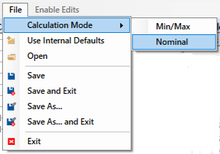 This feature turns off all tolerances in the component family Calculators to greatly simplify the data entry. 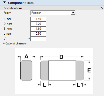 The Nominal Calculator has preset solder joint goals that have a fixed Toe, Heel and Side value. All solder joint goal values are editable for you to customize to meet your assembly shop guidelines for maximum quality in assembly attachment. The IPC J-STD-001 standard was used to derive the Footprint Expert Nominal Calculation Mode solder joint goals. You can use the mfr. recommended pattern or the internal solder joint goals. However, if you rely on component manufacturer tolerances and do not use the mfr. recommended patterns, we recommended that you use the IPC min/max mode for all your footprint and pad stack calculations. Just be aware that most package tolerances are not realistic. You need to understand which tolerances are too robust and tome them down to more realistic values. Note: if you use the Nominal Calculation Mode and save the data to an FPX Library, if you switch back to min/max calculation mode, the values saved to FPX will open in the calculator as nominal dimensions (without tolerances). If you open a min/max footprint from an FPX file library in the Nominal Calculation Mode, the tolerances will be removed and only the nominal package dimensions will display. |
|
|
|
|
Post Reply
|
|
| Tweet |
| Forum Jump | Forum Permissions You cannot post new topics in this forum You cannot reply to topics in this forum You cannot delete your posts in this forum You cannot edit your posts in this forum You cannot create polls in this forum You cannot vote in polls in this forum |


 Topic Options