|
|
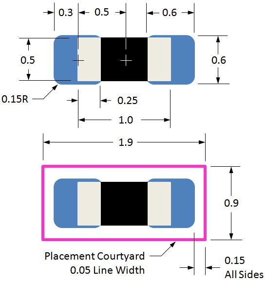
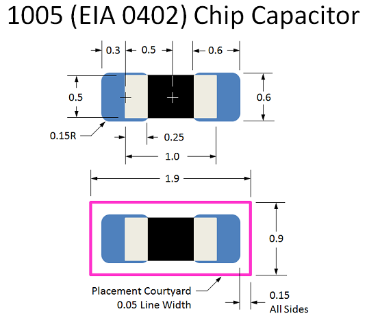
0402 Min Size Land Pattern |
Post Reply 
|
Page 12> |
| Author | |
wolfeman 
New User 

Joined: 19 Mar 2012 Status: Offline Points: 2 |
 Post Options Post Options
") Thanks(0) Thanks(0)
 Quote Reply Quote Reply
 Topic: 0402 Min Size Land Pattern Topic: 0402 Min Size Land PatternPosted: 19 Mar 2012 at 11:58am |
|
I have a design with 1mm & .8mm pitch BGAs on it. Using 0402 caps on back. Question, does anyone have any input with problems etc using 0402 patterns created using the smallest pattern calculated with current calculator? If I use smallest pattern 0402 it calculates out to about .56mm sq pads on .84mm centers. The 1mm BGA works reasonably well with this size 0402 and with gaps in balls on the .8mm part that smallest pattern could work well too. Any feedback will help. We really can’t switch to 0201s on this project at this time. Thanks Bob |
|
 |
|

|
|
|
|
|
Tom H
Admin Group 

Joined: 05 Jan 2012 Location: San Diego, CA Status: Offline Points: 6074 |
Post Options
Thanks(1)
Quote Reply
Posted: 19 Mar 2012 at 1:28pm |
|
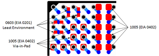
Bob, You’re on
the right track. Use the “Least” environment for EIA 0402 (1005 metric) chip
components. No one should ever use the Most environment for this chip size
due to excessive solder. If you
normally use the “Most” environment for library construction, use the “Nominal”
environment for the 0402 (1005) land pattern. If you
normally use the “Nominal” environment for library construction, use the
“Least” environment for the 0402 (1005) land pattern. Too much solder on this micro-miniature 2-pin component causes tombstoning in the assembly reflow oven (especially when using lead-free solder).
|
|
|
|
|
mypal_suresh
New User
Joined: 08 Oct 2014 Status: Offline Points: 1 |
Post Options
Thanks(0)
Quote Reply
Posted: 09 Oct 2014 at 8:26am |
|
Hello Tom, 1.In what all packages we should provide "Terminal " Dimesions as nominal instead of min and max. (ex:0201,0402,0603,0805 packages) 2.Can you be more specific to what is unrealistic tolerances ? In the above attached datasheet link the terminal dimesion is 0.3 +/- 0.1 mm. What would be T min and T max ? http://www.mouser.com/ds/2/40/cx7r-218113.pdf In this datasheet the terminal size 0.25 +/- 0.15 mm . What would be T min and T max ? Thanks in Advance
Regards
Sureshbabu |
|
|
|
|
Tom H
Admin Group
Joined: 05 Jan 2012 Location: San Diego, CA Status: Offline Points: 6074 |
Post Options
Thanks(0)
Quote Reply
Posted: 09 Oct 2014 at 9:19am |
|
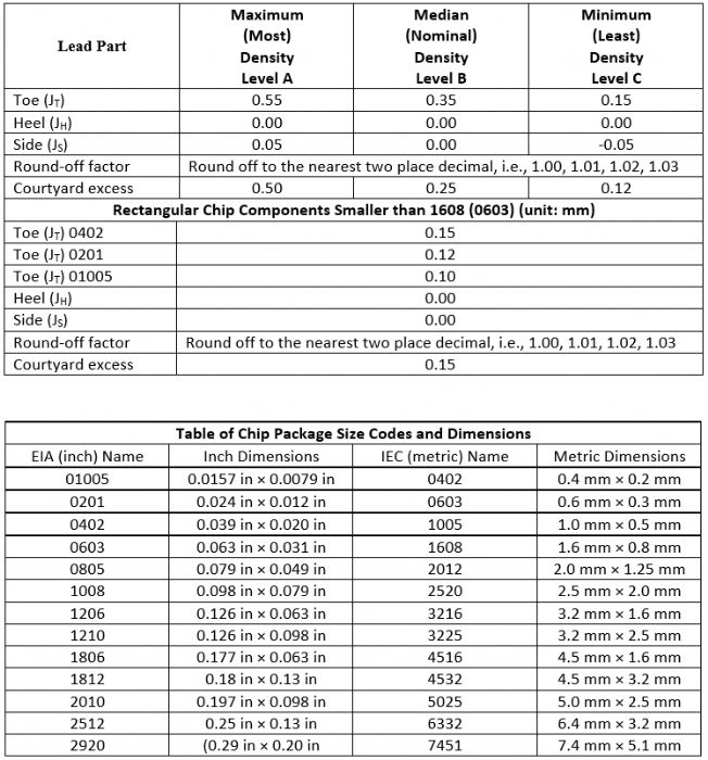
We had a meeting with IPC-7351 committee last week and we adjusted the "TOE" solder joint goal for parts less than 1.6 mm length. So I have to delete the comment about using only Nominal dimensions for the component terminal because we fixed that in the IPC Calculator in the V2014.11 release. Here is the new solder joint goal chart for chip components. These new values for miniature parts will eliminate tombstoning issues and provide the best paste volume for the assembly process.
|
|
|
|
|
Tom H
Admin Group
Joined: 05 Jan 2012 Location: San Diego, CA Status: Offline Points: 6074 |
Post Options
Thanks(0)
Quote Reply
Posted: 09 Oct 2014 at 9:21am |
|
I highly recommend that you download this new paper on Surface Mount Components - http://www.pcblibraries.com/forum/surface-mount-component-families_topic1391.html This paper provides the latest component families and terminal types and their related solder joint goal tables. |
|
|
|
|
Fynjy
New User
Joined: 06 Feb 2015 Status: Offline Points: 1 |
Post Options
Thanks(0)
Quote Reply
Posted: 06 Feb 2015 at 12:21am |
|
Hello Tom.
How will change the designation CAPC1608X90 if I use the density of A, B, C? |
|
|
|
|
Tom H
Admin Group
Joined: 05 Jan 2012 Location: San Diego, CA Status: Offline Points: 6074 |
Post Options
Thanks(0)
Quote Reply
Posted: 06 Feb 2015 at 7:24am |
|
The 1608 is the smallest chip that has 3-Tier Environment Density Levels Least, Nominal and Most).
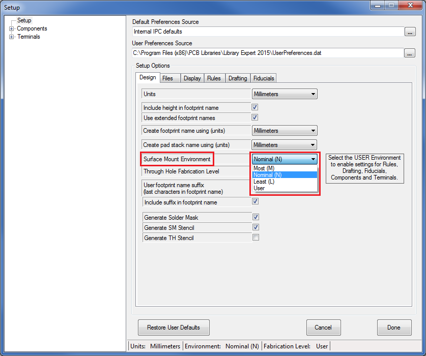
It depends on which version of Library Expert you are using (Pro or Lite) as to where you change the Environment. If you are using Library Expert Lite you change the Environment in the "Terminal > Environment" tab. If you are using Library Expert Pro you change the Environment in "Setup Preferences > User Preferences > Design > Surface Mount Environment > Drop Down" -
|
|
|
|
|
SandroLanot
New User
Joined: 11 Feb 2015 Status: Offline Points: 13 |
Post Options
Thanks(0)
Quote Reply
Posted: 11 Feb 2015 at 2:55pm |
|
Hi, This is my 1st post after joining few days ago. Is there any assembly attachment issues if my 0402 land pattern is 0.40 mm x 0.50 mm, with 1.00 mm pitch?
|
|
|
|
|
Tom H
Admin Group
Joined: 05 Jan 2012 Location: San Diego, CA Status: Offline Points: 6074 |
Post Options
Thanks(1)
Quote Reply
Posted: 11 Feb 2015 at 3:06pm |
|
Your pad size is the Least Environment. This is good for Nominal.
|
|
|
|
|
jayx
New User
Joined: 29 Mar 2015 Status: Offline Points: 7 |
Post Options
Thanks(0)
Quote Reply
Posted: 29 Mar 2015 at 2:19pm |
|
Hello,
I was trying to find recommended land pattern design for the most popular packages like 0603, 0805, SO8 etc. but it turns out to be pretty difficult. I found IPC-7351 and its 3-Tier approach but don’t really understand how can I calculate correct pad sizes using these values. Also I've seen PCB Library Expert SMD Reference Calculator but it returns incorrect values - try to enter 1608 (EIA 0603) package dimensions L=1.6, T=0.35, W=0.3 with ±0.15mm tolerance as found in Kemet datasheet http://www.kemet.com/Lists/ProductCatalog/Attachments/351/KEM_CC103_AUTO_SMD.pdf and calculated pads will overlap. Finally I've found information that ModelSource libraries available to download for DesignSpark are created to the IPC-7351 standard. However supposedly also based on IPC-7351 Kemet land pattern design recommendations in document mentioned above (page 12) is slightly different than these in ModelSource. By the way Kemet recommendations are also slightly different for 1005 (EIA 0402) than these in this topic. I know the differences are not big and in real life probably doesn’t matter but would be nice to keep land patterns the same across the industry. So I'm really surprised there are no exact dimensions specified e.g. in IPC-7351 for the most popular packages. |
|
|
|
|
Post Reply
|
Page 12> |
| Tweet |
| Forum Jump | Forum Permissions You cannot post new topics in this forum You cannot reply to topics in this forum You cannot delete your posts in this forum You cannot edit your posts in this forum You cannot create polls in this forum You cannot vote in polls in this forum |


 Topic Options