 LOGIN
LOGIN Downloads


The process of importing footprints from PCB Footprint Expert into Altium Circuit Studio can be a little counterintuitive. Here is a step by step guide to getting it done.
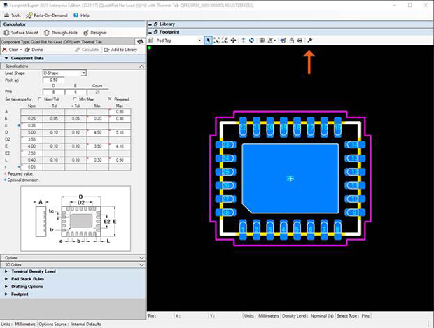
1. Open an FPX file or design your footprint in the PCB Footprint
Expert. When you are finished, click the Build Footprint button
indicated by the arrow below.
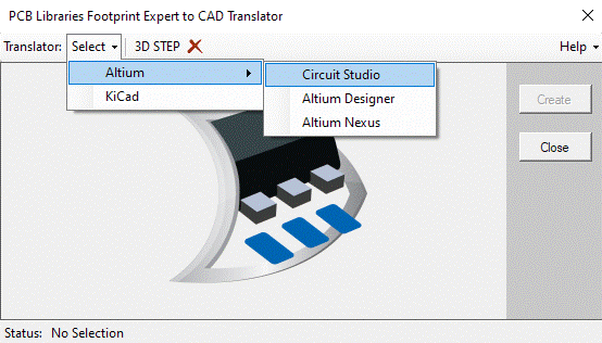
2. The translator dialog will pop up. Click Select,
and choose Altium > Circuit Studio. If you don't see anything in this dialog or
the Circuit Studio option is missing, this means that you are not currently
licensed to export to this format.
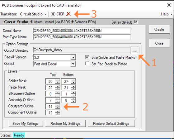
3. First select an output directory, You can then
adjust any of the layer settings, Change Courtyard Outline to 14, then
click on the 3D STEP button.
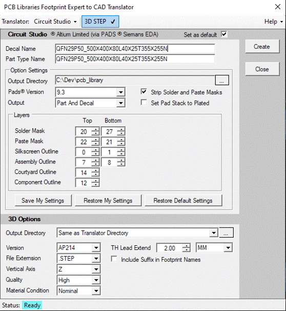
4. The 3D options will appear. Once again, the default settings
work well. Click on Create and your footprint will be
exported to disk.
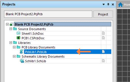
5. At this point, you need to have a Circuit Studio project in
progress. If you don't already have your own PCB Library, create
one now.
6. Click File > Import and browse to the folder where
you exported your footprint files from PCB Footprint Expert.

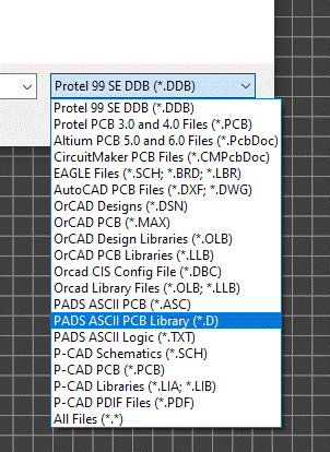
7. Change the file type filter in the lower right
corner of the file dialog to PADS files.
8. Select the file that you want to import, and click Open.
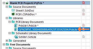
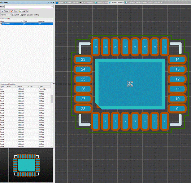
9. You should now see the new footprint appear as a new library
in your project browser. However we don't want a new library with
a solitary footprint in it. Double click the new library to open it.
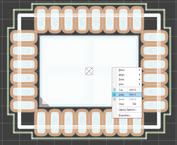
10. Select the footprint and copy it. Don't forget that you must click on the selected
footprint after the copy command or the copy won't be performed!
11. Navigate back to your own footprint library and create a new
blank footprint with an appropriate name. Inside the drawing
area, paste the copied footprint and place it on [0,0].
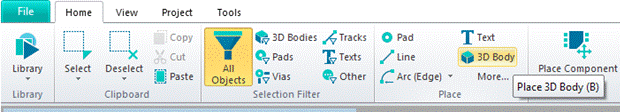
12. Click on the Home tab and click: 3D body.
Navigate to where you exported your footprint from PCB Footprint
Expert and choose the appropriate .STEP file.
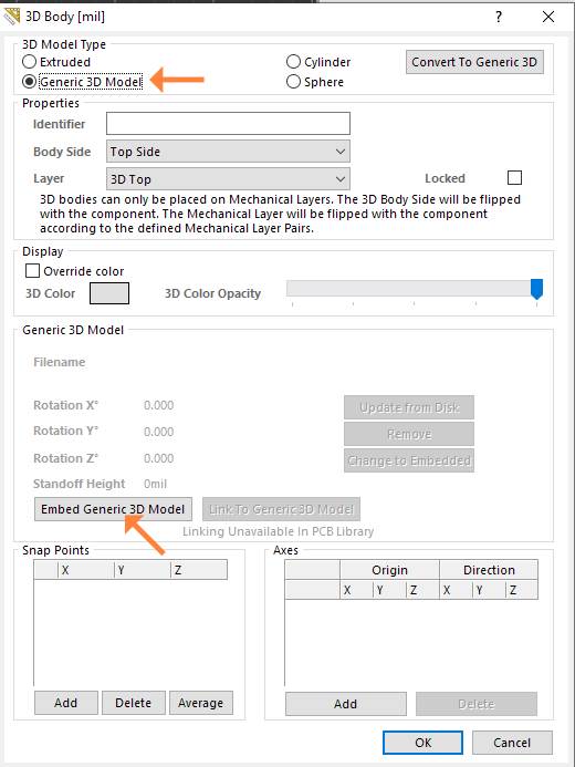
13. In the next dialog, select Generic 3D Model then
press the Embed Generic 3D Model. Press OK.
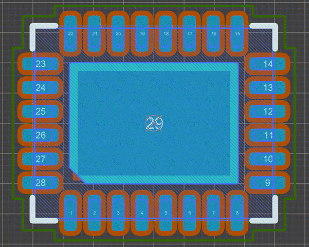
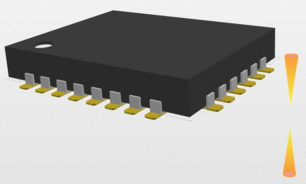
14. Click on the center of your footprint to drop the 3D model onto your footprint. It should show as a blue hatched area.
15. Finally, check that everything is matching and your footprint
and STEP model looks correct in 3D. Click the View tab,
then choose Switch to 3D to view your footprint in 3D.
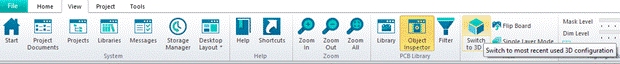
Hint - to navigate around the 3D viewport, hold Shift then Right-click drag on the little ball gizmo that appears.
Now your new footprint is ready to be assigned to your schematic library components.
You can now delete the un-needed imported PCB Library (from Step 3).